Enhanced brightness light emitting device spot emitter

a light emitting device and spot emitter technology, applied in the direction of discharge tube/lamp details, discharge tube luminescnet screens, lighting and heating apparatus, etc., can solve the problems of low light generating efficiency, high current density, and increased lens cost, so as to increase the amount of usefully captured light in the optical system

Inactive Publication Date: 2005-11-29
LUMILEDS
View PDF10 Cites 63 Cited by
  • Summary
  • Abstract
  • Description
  • Claims
  • Application Information

AI Technical Summary

Benefits of technology

[0009]In accordance with embodiments of the invention, the amount of usefully captured light in an optical system may be increased by concentrating light in a region where it can be collected by the optical system.

Problems solved by technology

However, as the diameter of a lens increases, the cost of the lens increases.
However, the efficiency of light emitting diodes usually falls at high current densities due to, for example, heating effects, saturation in the light emitting layers of the charge carriers that recombine to produce light, or the loss of confinement of the charge carriers that recombine to produce light.
The loss of light generating efficiency at high current density limits the amount of light generated per unit area that can be created in a light emitting diode.

Method used


Image

  • Enhanced brightness light emitting device spot emitter
  • Enhanced brightness light emitting device spot emitter
  • Enhanced brightness light emitting device spot emitter

Examples


Embodiment Construction

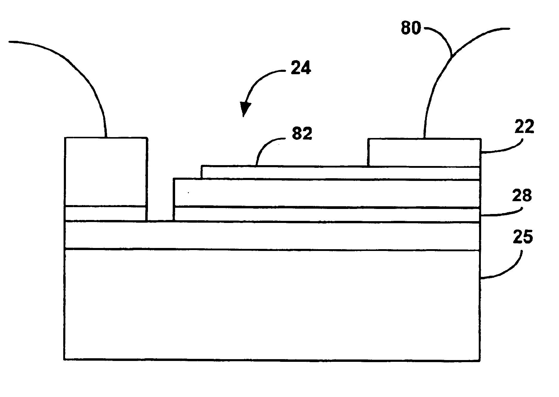
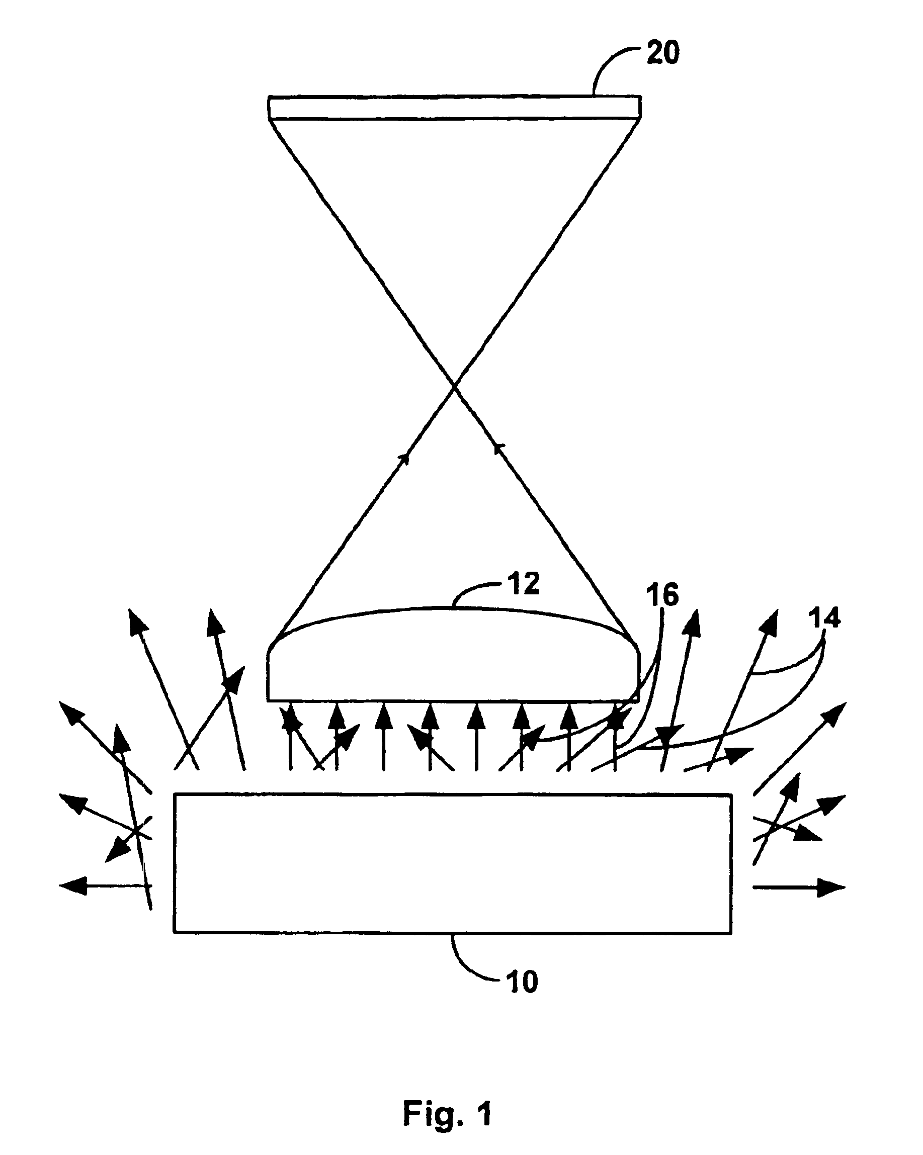
[0024]In accordance with embodiments of the invention, the amount of light captured in an optical system may be increased by directing light from the source into the etendue-limit of the optical system so that it can be captured by the optical system. The light source may be a semiconductor light emitting device such as a light emitting diode. Embodiments of the invention are applicable to semiconductor light emitting devices of various materials systems, including, for example, III-V systems such as III-nitride, III-phosphide, and III-arsenide, and II-VI systems. Further, embodiments of the invention are applicable to any semiconductor light emitting devices where the device layers and substrate are reasonably transparent to light, including devices having both contacts formed on the same side of the device, such as flip-chip and epitaxy-up devices, as well as devices having contacts formed on opposite sides of the device.

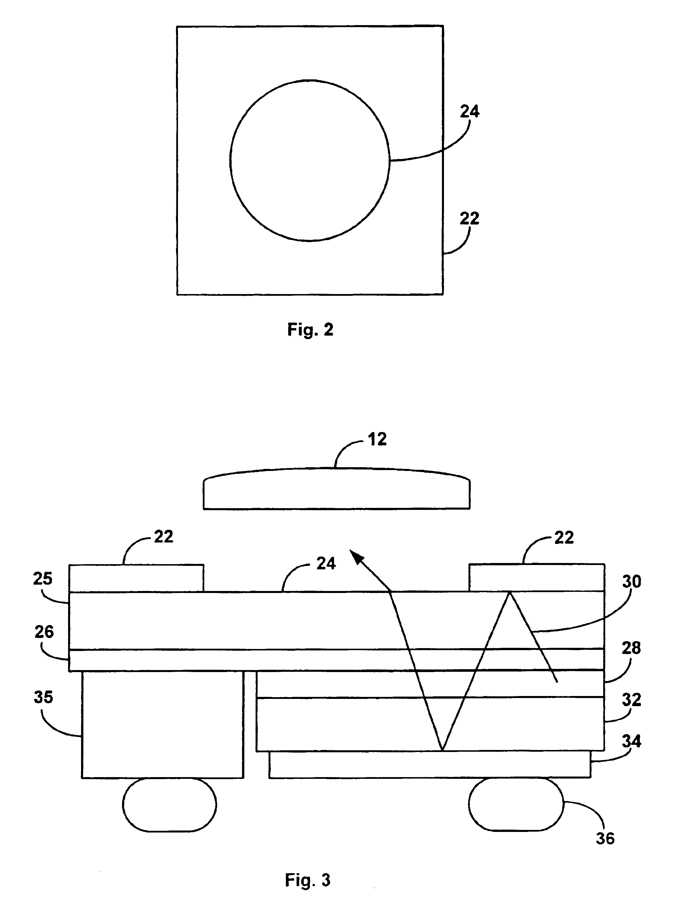
[0025]FIG. 2 illustrates a top view of a light emitting devi...


PUM


Abstract

The amount of usefully captured light in an optical system may be increased by concentrating light in a region where it can be collected by the optical system. A light emitting device may include a substrate and a plurality of semiconductor layers. In some embodiments, a reflective material overlies a portion of the substrate and has an opening through which light exits the device. In some embodiments, reflective material overlies a portion of a surface of the semiconductor layers and has an opening through which light exits the device. In some embodiments, a light emitting device includes a transparent member with a first surface and an exit surface. At least one light emitting diode is disposed on the first surface. The transparent member is shaped such that light emitted from the light emitting diode is directed toward the exit surface.

Description

CROSS REFERENCE TO RELATED APPLICATIONS[0001]This application is a Division of U.S. patent application Ser. No. 10 / 283,737, filed on Oct. 29, 2002, now U.S. Pat. No. 6,730,940, which is incorporated herein by reference.BACKGROUND[0002]1. Field of Invention[0003]The present invention relates generally to increasing the brightness of a light emitting diode light source.[0004]2. Description of Related Art[0005]FIG. 1 illustrates a lens 12 transmitting light generated by a light source 10 such as a light emitting diode. A key issue in designing light sources to be used with optical systems comprised of passive optical imaging elements, such as lens 12, is illustrated in FIG. 1. Only light emitted from the source area that is consistent with the optical invariant or etendue of lens 12 can be usefully focused onto the target area 20 (for example, a transparent microdisplay). The etendue of a given optical system is defined as:E=∫∫(cos θ)dAdΩ  (1)where θ is the angle between the normal to ...

Claims


Application Information

Patent Timeline
Patent Type & Authority Patents(United States)
IPC IPC(8): H01L33/46H01L33/58H01L33/60
CPCH01L33/46H01L33/58H01L33/60
Inventor STERANKA, FRANK M.STEIGERWALD, DANIEL A.KEUPER, MATTHIJS H.
Owner LUMILEDS
Why Eureka
Try Eureka