Optical memory and logic using cross-switches

a logic and optical memory technology, applied in the field of optical memory, can solve the problems of not being very small and randomly accessible to fiber delay lines

Inactive Publication Date: 2005-11-08
LOCKHEED MARTIN CORP
View PDF8 Cites 8 Cited by
  • Summary
  • Abstract
  • Description
  • Claims
  • Application Information

AI Technical Summary

Benefits of technology

[0007]The present invention provides for all-optical random access memory (buffer) and all-optical logic, which is necessary for all-optical computing and all-optical networks. The present invention uses optically-induced total internal reflection to achieve all-optical switching, logic and memory functions. Devices based on the cross-switches employed in the present invention require no electronic biasing and are very compact. The present all-optical memory cell is randomly accessible.

Problems solved by technology

Fiber delay lines are not randomly accessible nor are they very small.

Method used


Image

  • Optical memory and logic using cross-switches
  • Optical memory and logic using cross-switches
  • Optical memory and logic using cross-switches

Examples


Embodiment Construction

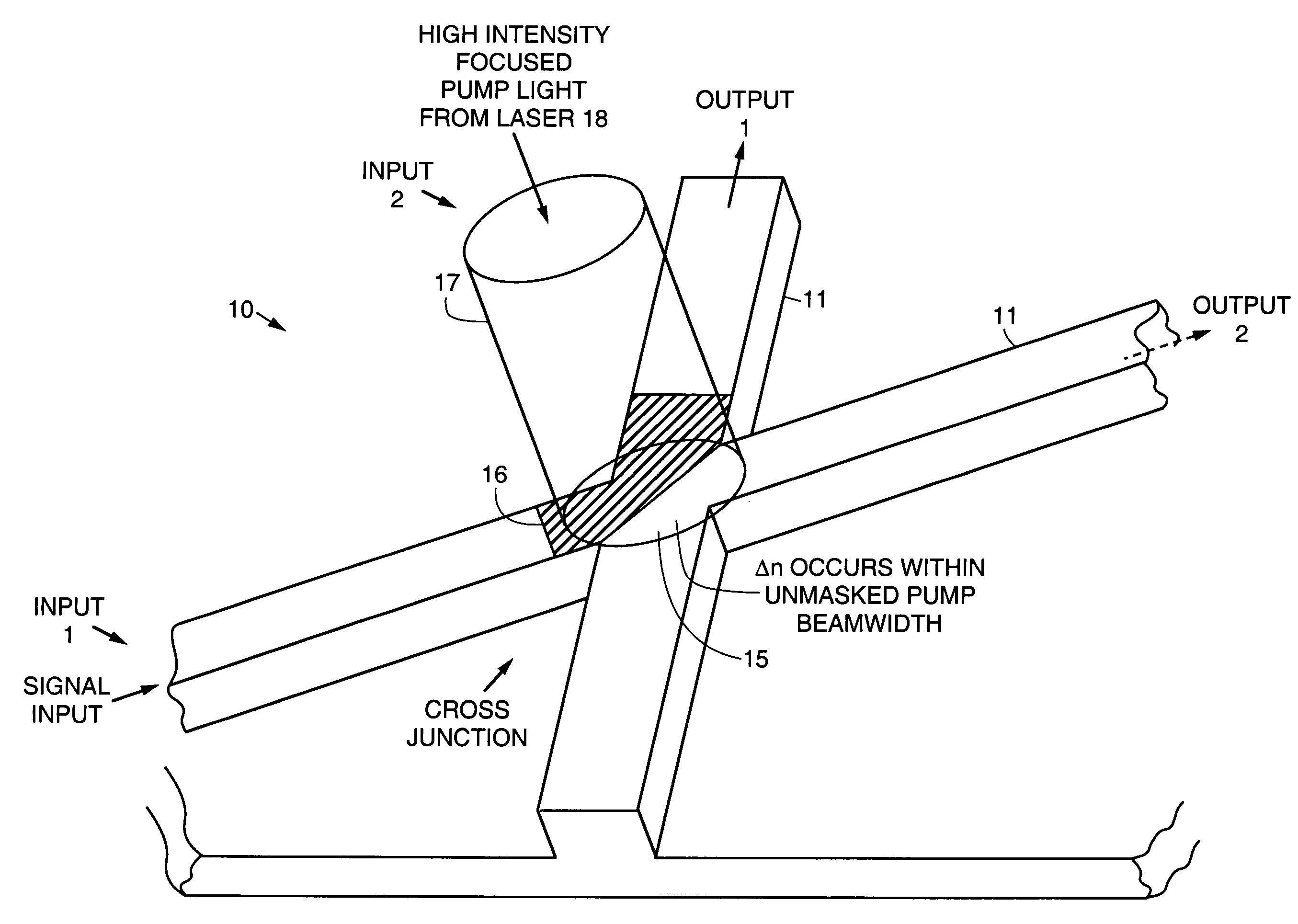
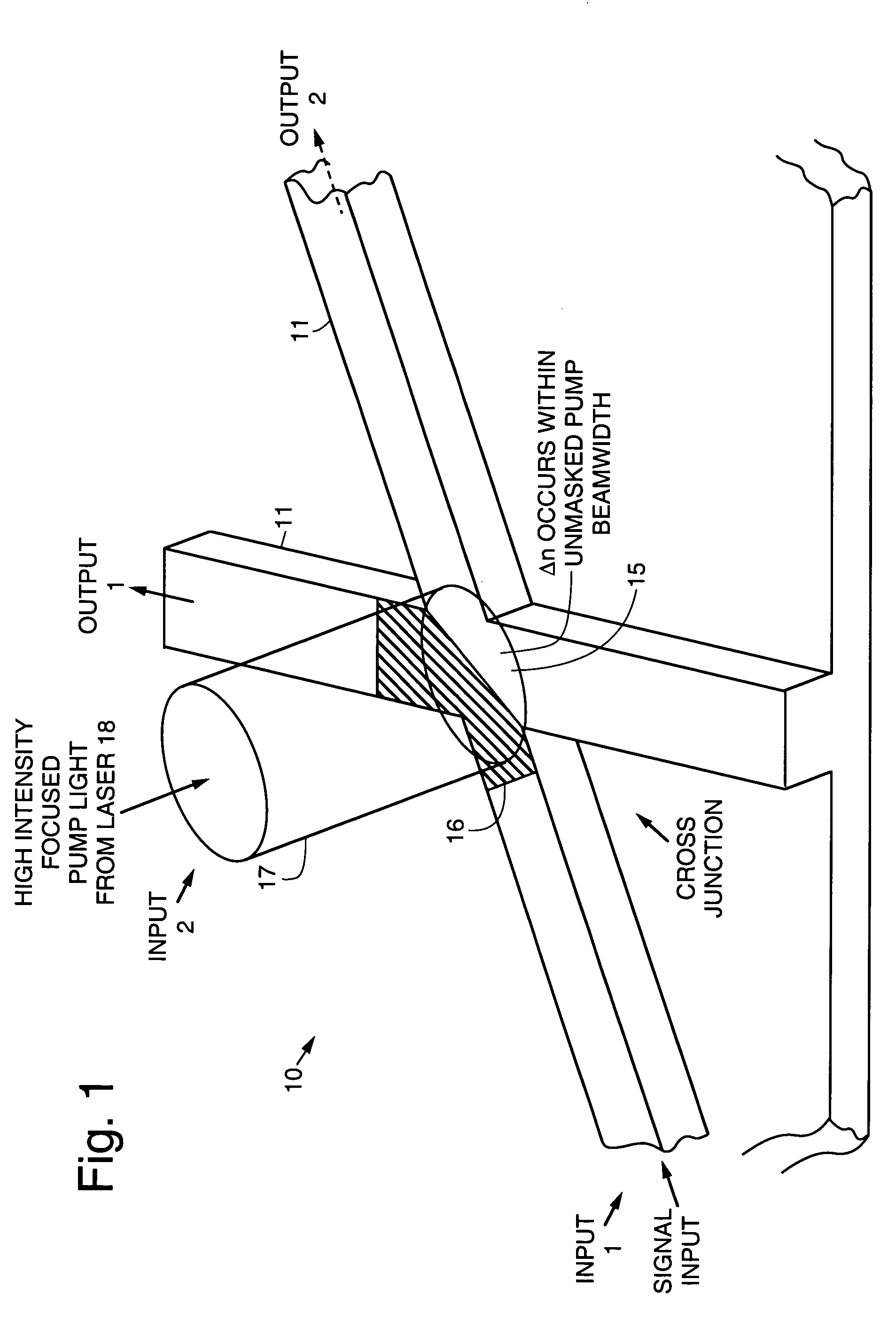
[0024]Referring to the drawing figures, FIG. 1 illustrates an exemplary cross-switch 10 in accordance with the principles of the present invention when observed at an oblique angle. The exemplary cross-switch 10 may be used to implement an all-optical, asynchronous binary storage cell, wherein the cross-switch 10 employs optically induced total internal reflection. The binary cell is a building block for a programmable all-optical random access memory (AORAM) device, which enables circuits and networks that require optical buffers.

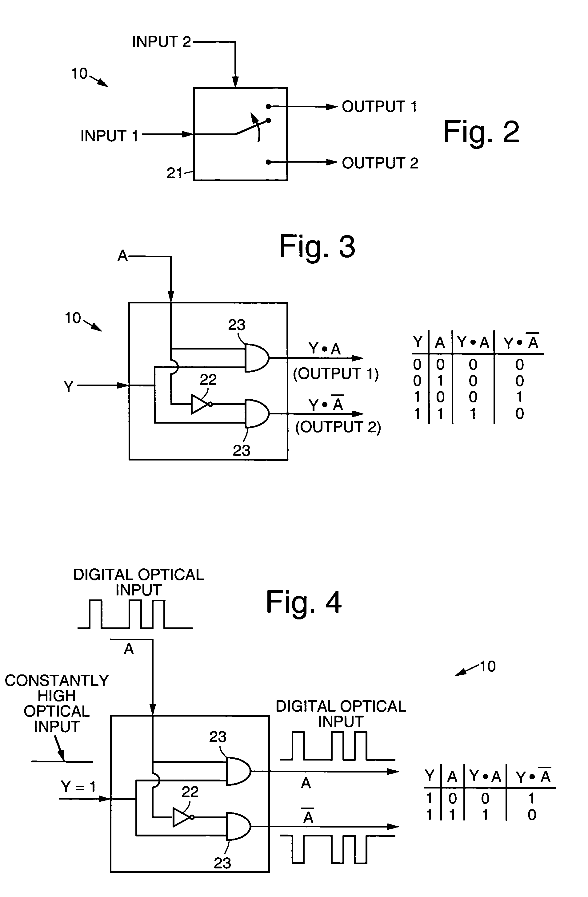
[0025]In order to simplify the definition of a binary memory cell, several logic gates and their functions are described below. Corresponding all-optical equivalent logic gates using cross-switches are also described. As defined herein, the term “all-optical” refers to the directing of optical data signals as a result of optical control signal inputs without the need for conversions between optical and electrical domains.

[0026]The all-optical switch 10 is ...


PUM

PropertyMeasurementUnit
total internal reflectionaaaaaaaaaa
optical outputaaaaaaaaaa
opticalaaaaaaaaaa

Abstract

An all-optical, asynchronous binary storage cell implemented by optically induced total internal reflection cross-junction waveguide switches. The term “all-optical” refers to directing of optical data signals as a result of optical control signal inputs without the need for conversion between optical and electrical domains. The binary cell is a building block for a programmable all-optical random access memory (AORAM) device. The AORAM device enables circuits and networks that require optical buffers.

Description

BACKGROUND[0001]The present invention relates generally to optical memory, and more particularly, to improved optical memory and logic using cross-switches.[0002]Conventional all-optical memory approaches include technologies based on fiber delay lines, semiconductor optical amplifiers, quantum dots, self-electro-optic effect devices, and gain-coupled lasers.[0003]Fiber delay lines are not randomly accessible nor are they very small. Semiconductor optical amplifiers, quantum dots, self-electro-optic effect devices and gain-coupled lasers all require electronic biasing. It would be advantageous to have optical memory and logic that improves upon these conventional approaches.[0004]It is an objective of the present invention to provide for improved optical memory and logic employing cross-switches. It is also an objective of the present invention to provide for an all-optical asynchronous binary memory cell and logic functions implemented with optically induced total internal reflecti...

Claims


Application Information

Patent Timeline
Patent Type & Authority Patents(United States)
IPC IPC(8): G02B6/26G02F3/00G11C13/04G02F1/315G02F1/35
CPCG02F1/3515G02F1/315G11C13/048
Inventor SPICKERMANN, RALPHSAKAMOTO, STEVEN R.
Owner LOCKHEED MARTIN CORP
Why Eureka
Try Eureka