Reprogrammable non-volatile memory using a breakdown phenomena in an ultra-thin dielectric

Inactive Publication Date: 2005-10-18
SYNOPSYS INC
View PDF40 Cites 62 Cited by
  • Summary
  • Abstract
  • Description
  • Claims
  • Application Information

AI Technical Summary

Problems solved by technology

With 10 volts, this thus results in a substantial amount of time for programming a memory cell.
However, the application of a write voltage to the electrode of the gate controlled diode causes the silicon dioxide / silicon nitride interface to fill with positive charge, which is retained after the write operation is completed.
Accordingly, processes for Flash devices tend to be one or two generations behind the standard advance CMOS logic process and about 30% more expensive on a cost-per-wafer basis.
While the antifuse is fabricated without the additional film manufacturing processes typically required for fabricating antifuse circuits, Tamura et al. encounter another problem.

Method used


Image

  • Reprogrammable non-volatile memory using a breakdown phenomena in an ultra-thin dielectric
  • Reprogrammable non-volatile memory using a breakdown phenomena in an ultra-thin dielectric
  • Reprogrammable non-volatile memory using a breakdown phenomena in an ultra-thin dielectric

Examples


Embodiment Construction

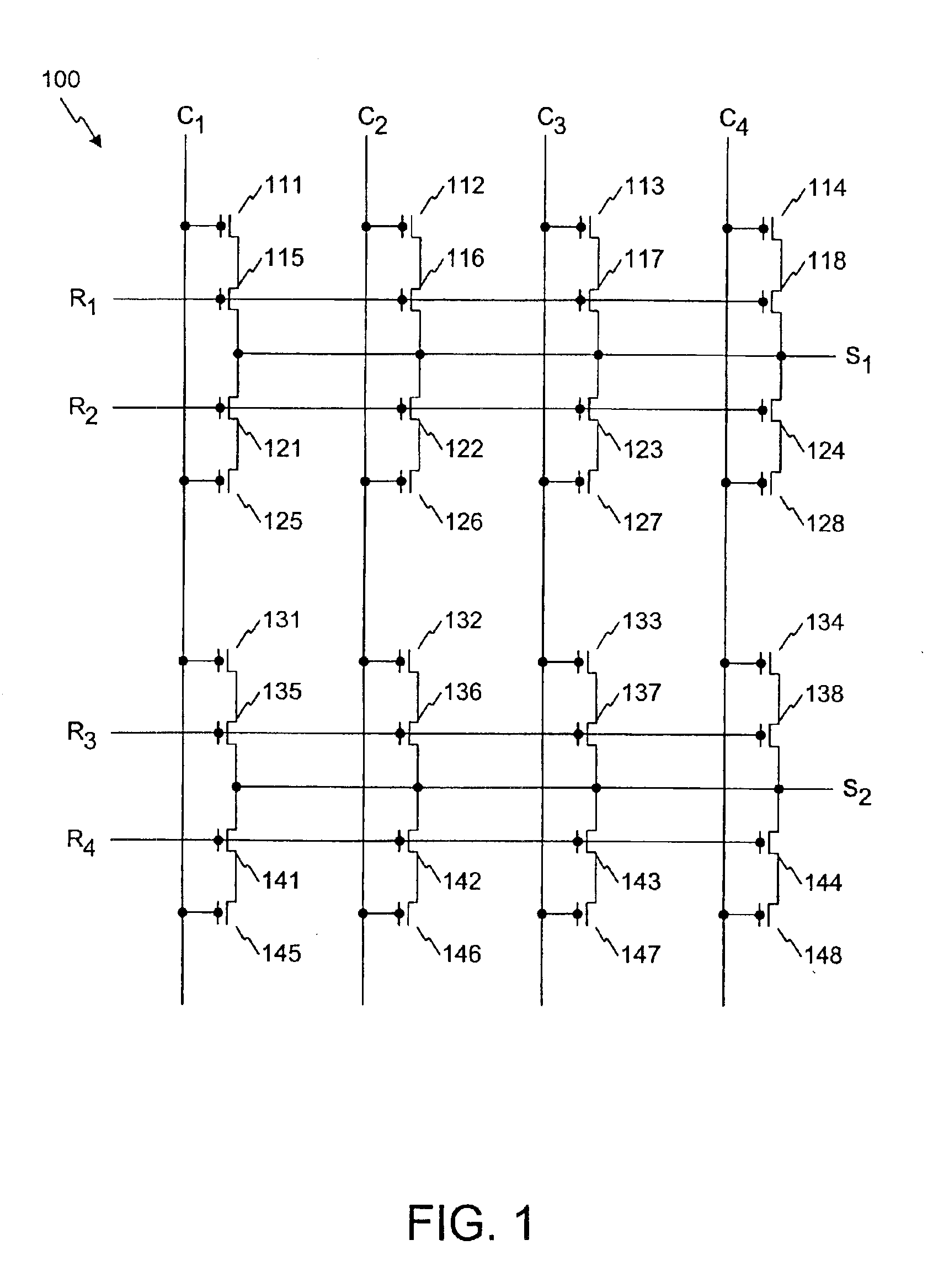
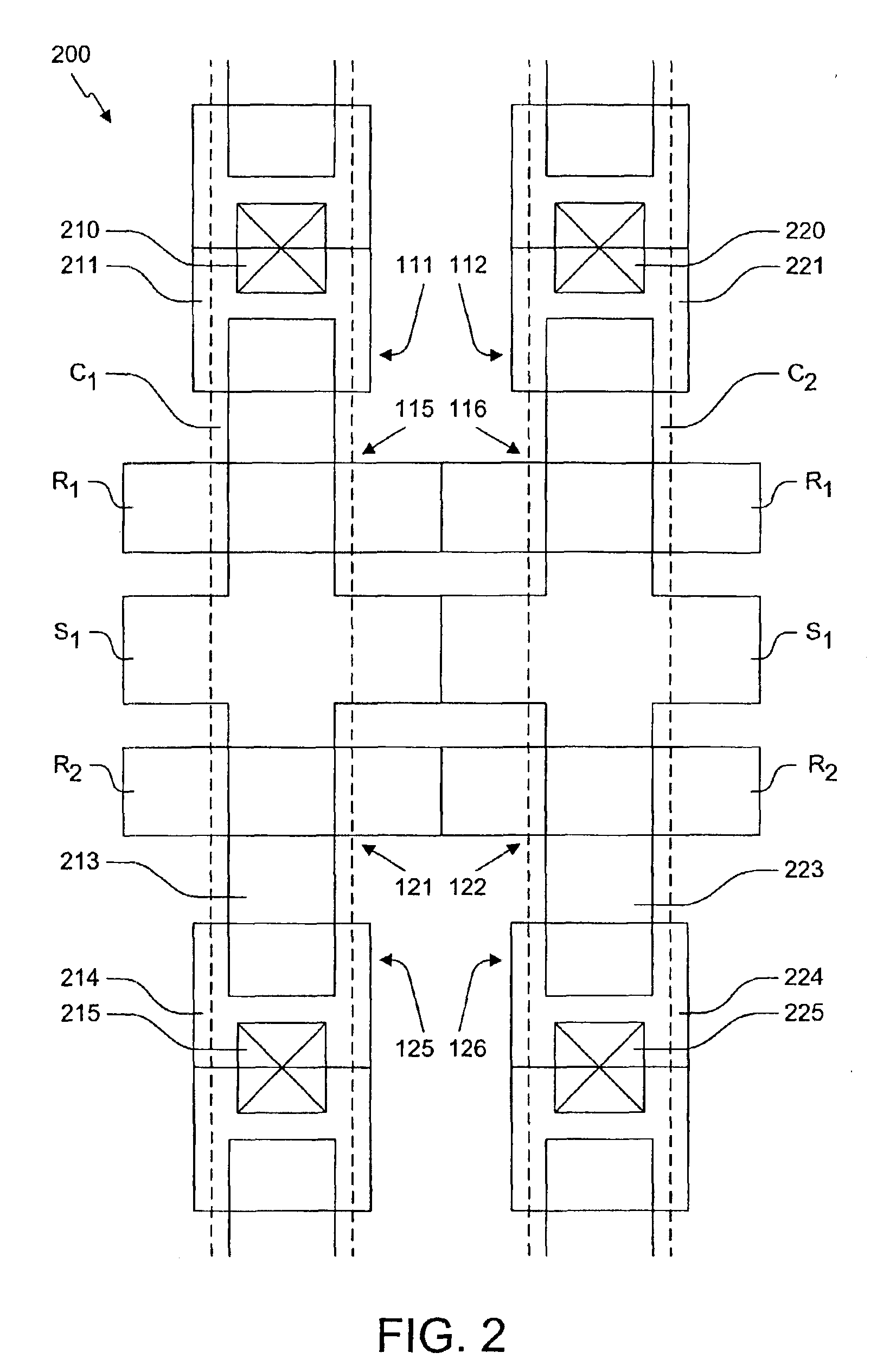
[0026]The present invention is a reprogrammable non-volatile memory cell and memory array. The non-volatile memory is comprised of semiconductor memory cells having a data storage element constructed around an ultra-thin dielectric, such as a gate oxide, used to store information by stressing the ultra-thin dielectric into breakdown (soft or hard breakdown) to set the leakage current level of the memory cell. The memory cell is read by sensing the current drawn by the cell. A suitable ultra-thin dielectric is, for example, high quality gate oxide of about 50 Å thickness or less, as is commonly available from presently available advanced CMOS logic processes, for example. Such oxides are commonly formed by deposition, by oxide growth from a silicon active region, or by some combination thereof. Other suitable dielectrics include oxide-nitride-oxide composites, compound oxides, and so forth.

[0027]The memory cells are reprogrammable by increasing the magnitude of dielectric breakdown f...


PUM


Abstract

A reprogrammable non-volatile memory array and constituent memory cells is disclosed. The semiconductor memory cells each have a data storage element constructed around an ultra-thin dielectric, such as a gate oxide. The gate oxide is used to store information by stressing the ultra-thin dielectric into breakdown (soft or hard breakdown) to set the leakage current level of the memory cell. The memory cell is read by sensing the current drawn by the cell. A suitable ultra-thin dielectric is high quality gate oxide of about 50 Å thickness or less, as commonly available from presently available advanced CMOS logic processes. The memory cells are first programmed by stressing the gate oxide until soft breakdown occurs. The memory cells are then subsequently reprogrammed by increasing the breakdown of the gate oxide.

Description

RELATED APPLICATION[0001]The present application hereby claims priority under 35 U.S.C. 120 and is divisional from U.S. patent application Ser. No. 09 / 995,641 filed Sep. 18, 2001 entitled “SEMICONDUCTOR MEMORY CELL AND MEMORY ARRAY USING A BREAKDOWN PHENOMENA IN AN ULTRA-THIN DIELECTRIC” and is a division of U.S. Pat. application Ser. No. 09 / 982,314 filed Oct. 17, 2001, now U.S. Pat. No. 6,700,151, REPROGRAMMABLE NON-VOLATILE MEMORY USING A BREAKDOWN PHENOMENA IN AN ULTRA-THIN DIELECTRIC.TECHNICAL FIELD OF THE INVENTION[0002]The present invention relates to reprogrammable non-volatile memory, and more particularly, to a non-volatile reprogrammable semiconductor memory that uses a breakdown phenomena in an ultra-thin dielectric such as a MOS gate dielectric to store digital information.BACKGROUND OF THE INVENTION[0003]Non-volatile memory retains stored data when power is removed, which is required or at least highly desirable in many different types of computers and other electronic ...

Claims


Application Information

Patent Timeline
IPC IPC(8): H01L27/112H01L21/70H01L21/8246H01L27/10H01L29/94
CPCH01L27/112H01L27/11206H01L29/94H10B20/20H10B20/00
Inventor PENG, JACK ZEZHONG
Owner SYNOPSYS INC
Why Eureka
Try Eureka