Microfluidic devices for introducing and dispensing fluids from microfluidic systems
- Summary
- Abstract
- Description
- Claims
- Application Information
AI Technical Summary
Benefits of technology
Problems solved by technology
Method used
Image
Examples
example 1
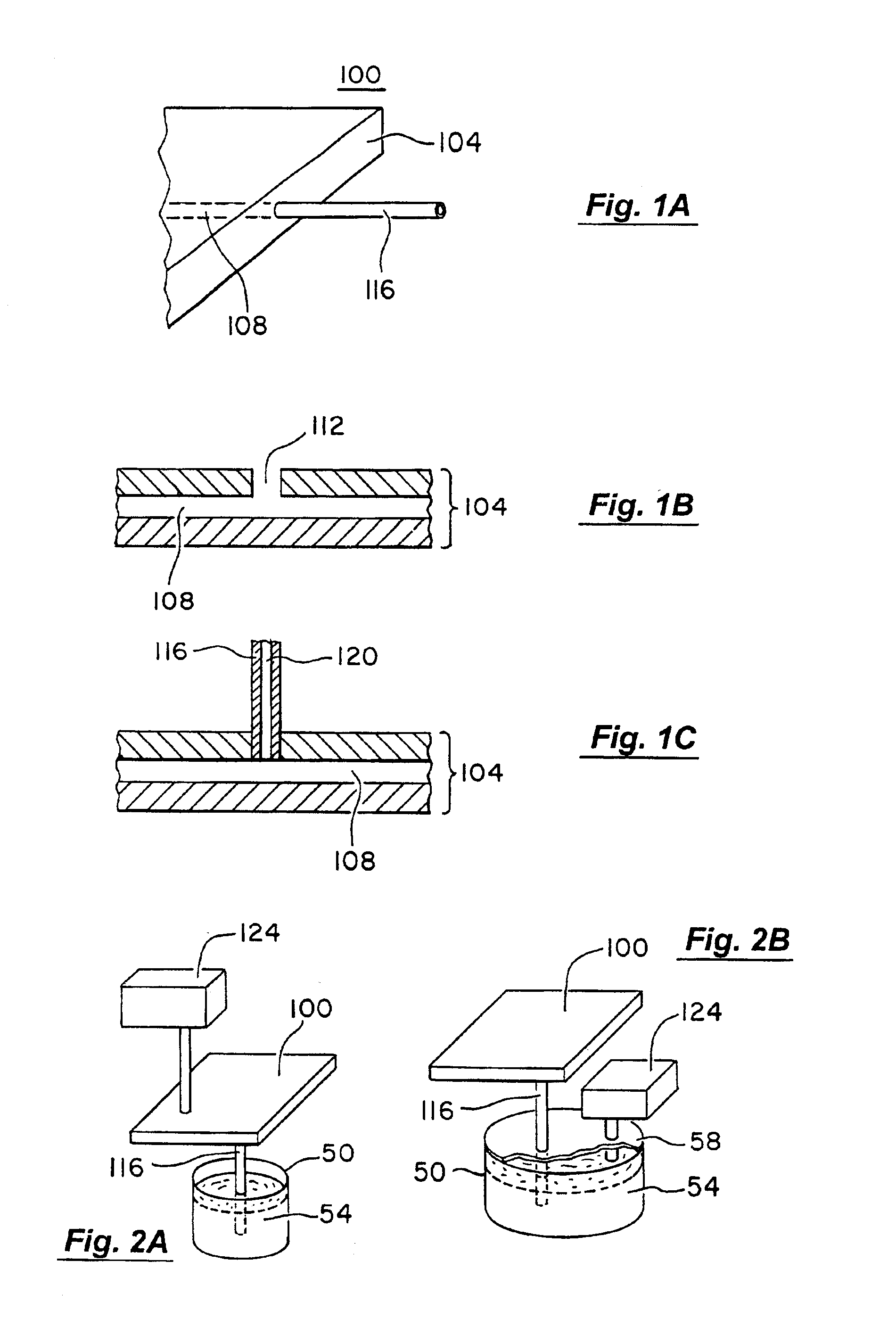
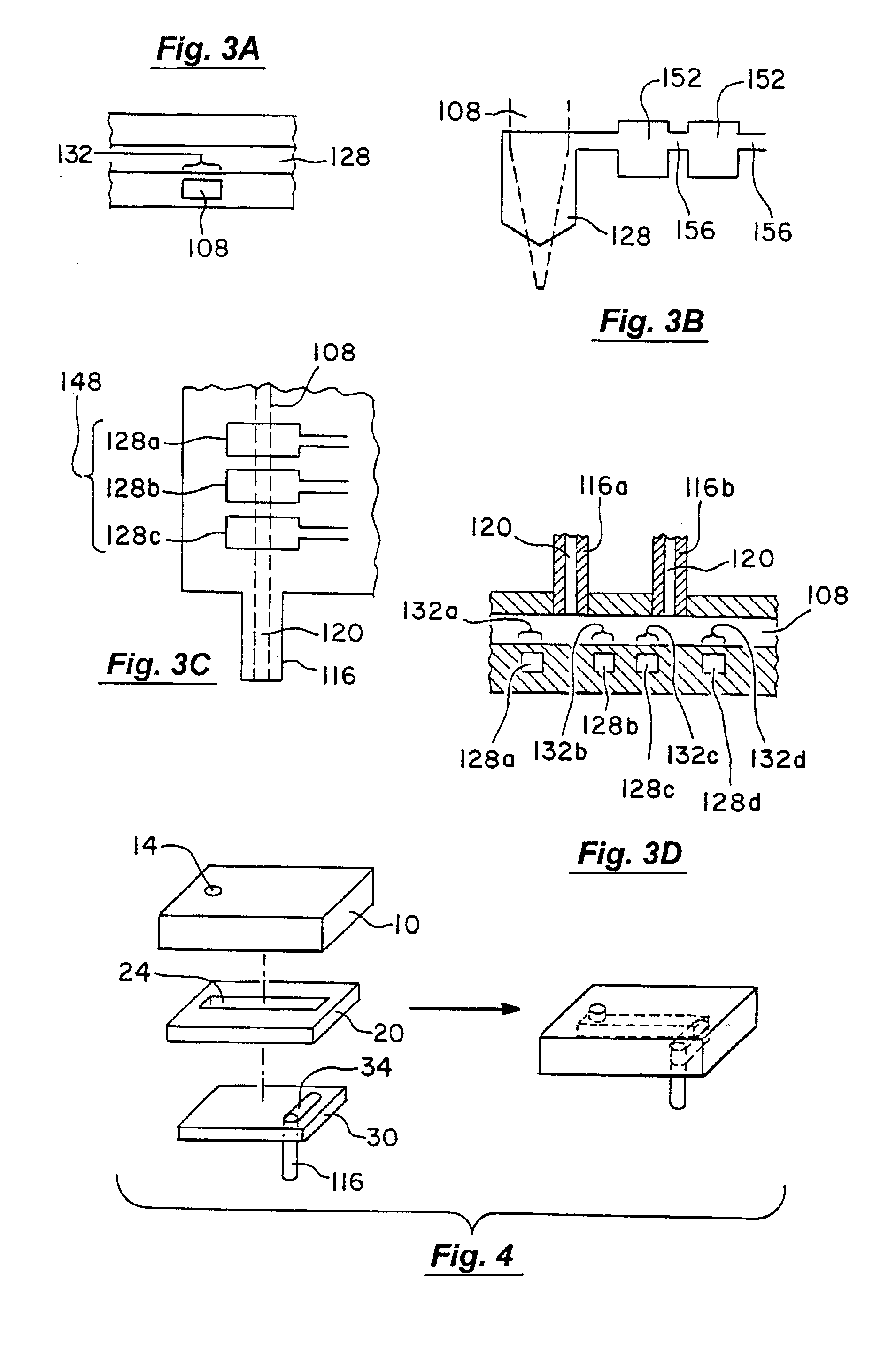
[0258]This example illustrates a three-layer fabrication process for producing a microfluidic sipper.
[0259]Three silicon wafers were cleaned by washing with acetone, isopropyl alcohol (IPA), deionized (DI) water, IPA and drying with N2. The resulting wafers were dehydration baked on a hot plate at 100° C. for 5 minutes, cooled and treated with hexamethyldisilazane (HMDS) vapor for 10 minutes in a chamber. The wafers were then removed from the HMDS vapor chamber and spin coated with Shipley 5740 resist to produce a 10 μm layer. The resulting wafers were softbaked in a 90° C. oven for 1 hr, exposed to UV and developed in Shipley 2401 developer. The developed wafers were hard baked in a 150° C. oven for 1 hr to provide a rounded profile photoresist mold.
[0260]The molds were used to make the sipping device using a two component silicone rubber (GE RTV 615). The control layer, i.e., layer comprising the control channels, was made by mixing a 4:1 ratio of A:B components to produce a 4 mm ...
example 2
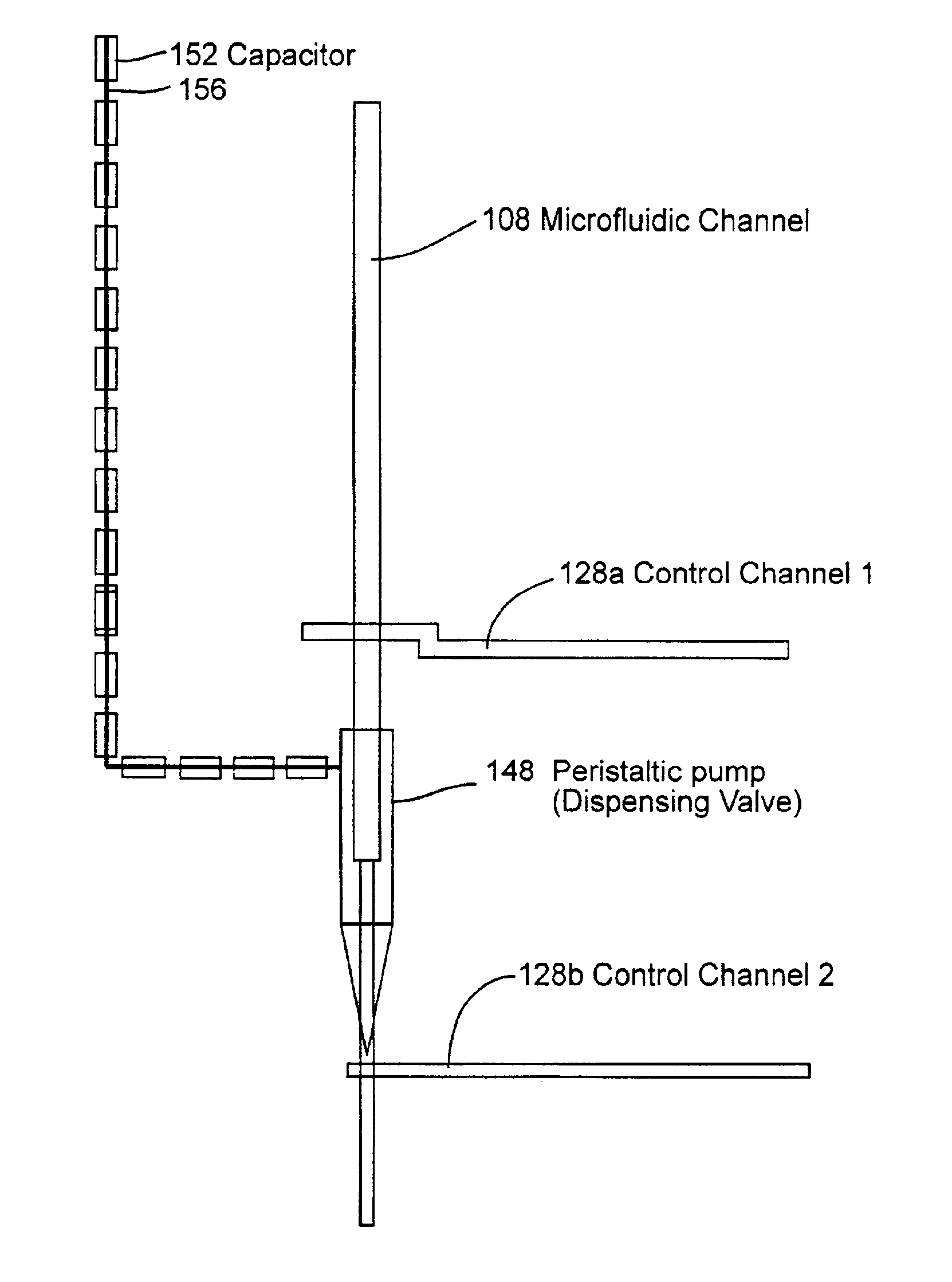
[0261]This example illustrates a three-layer fabrication process for producing a microfluidic dispenser.
[0262]Two silicon wafers were cleaned by washing with acetone, IPA, DI water, IPA and drying with N2. The wafers were then dehydration baked on a hot plate at 100° C. for 5 minutes, cooled and treated with HMDS vapor for 10 minutes. The wafers were removed from the HMDS vapor chamber and coated with Shipley 5740 resist spun to produce a 7 μm layer. The wafers were then softbaked in a 90° C. oven for 1 hr, exposed with UV and developed in Shipley 2401 developer. The developed wafers were hard baked on a 200° C. hotplate for 1 hr, cooled and placed in a HMDS vapor chamber for 10 minutes. AZ PLP 100XT resist was spun on the wafers to produce a 45 μm layer. The wafers were then soft baked at 90° C. for 1.5 hrs, cooled, exposed to UV, developed in AZ 400K developer and at 200° C.
[0263]The two layer portion of the PDMS chip was made using the process described in Science 7 April 2000, V...
example 3
[0265]This example illustrates a microfabrication process for producing a microfluidic dispenser containing a single line pump, i.e., one control channel peristaltic pump.
[0266]Two silicon wafers were cleaned by washing with acetone, IPA, DI water, IPA and drying with N2. The wafers were then dehydration baked on a hot plate at 100° C. for 5 minutes, cooled, treated with HMDS vapor and coated with AZ 5214-E resist spun to produce a 2 μm layer. The wafers were then softbaked on a 100° C. hotplate for 2 min, exposed to UV, developed in AZ 400K developer and hard baked on a 200° C. hotplate for a 1 hr. The wafers were cooled and treated with HMDS vapor for 10 minutes. AZ PLP 100XT resist was spun on to the wafers to produce a 45 μm layer. The wafer were then soft baked at 90° C. for 1.5 hrs, exposed to UV, developed in AZ 400K developer and hard-baked at 200° C.
[0267]The molds were then used to make a microfluidic device comprising a single control channel peristaltic pump using a two ...
PUM
 Abstract
Description
Claims
Application Information
 - R&D
- Intellectual Property
- Life Sciences
- Materials
- Tech Scout
- Unparalleled Data Quality
- Higher Quality Content
- 60% Fewer Hallucinations
Browse by: Latest US Patents, China's latest patents, Technical Efficacy Thesaurus, Application Domain, Technology Topic, Popular Technical Reports.
© 2025 PatSnap. All rights reserved.Legal|Privacy policy|Modern Slavery Act Transparency Statement|Sitemap|About US| Contact US: help@patsnap.com


