Method of forming buried conductors

Inactive Publication Date: 2005-09-20
MICRON TECH INC
View PDF45 Cites 24 Cited by
  • Summary
  • Abstract
  • Description
  • Claims
  • Application Information

AI Technical Summary

Benefits of technology

[0009]The use of a plurality of conductive elements buried within the substrate of a semiconductor structure overcomes limitations found in the prior art. For example, where each conductive element is a separate buried plane, there may be two or more such planes, such that a three-dimensional semiconductor structure may be formed. Three-dimensional structures, as those of ordinary skill within the art can appreciate, have the ability to significantly reduce the average distance from one segment of a large computer processor and associated memory to another, allowing for higher-density semiconductor storage devices and faster processors.

Problems solved by technology

As the number of wiring levels grew, the requirement of the vertical connections has significantly reduced the usefulness of the lower levels.
A limited prior art solution is to use a single buried wiring level in the initial phases of semiconductor fabrication.
A single buried wiring level overcomes the limitations of using external wiring planes, but is not entirely applicable to current semiconductor technology.

Method used


Image

  • Method of forming buried conductors
  • Method of forming buried conductors
  • Method of forming buried conductors

Examples


Embodiment Construction

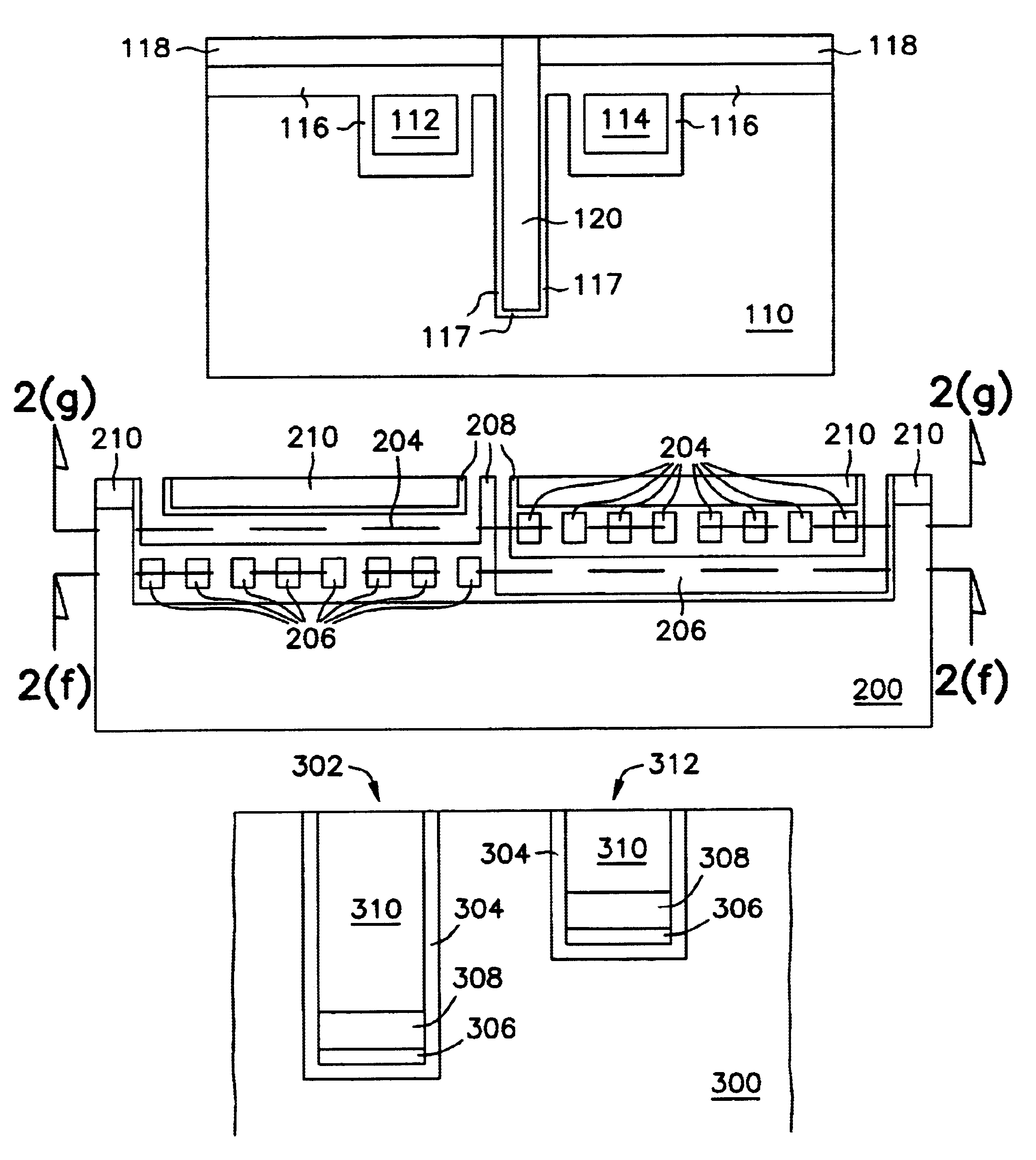
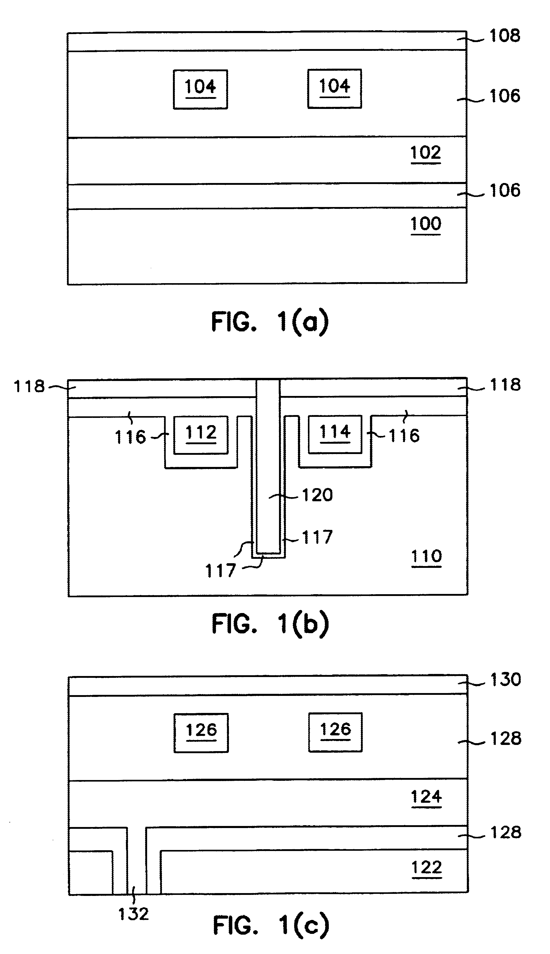
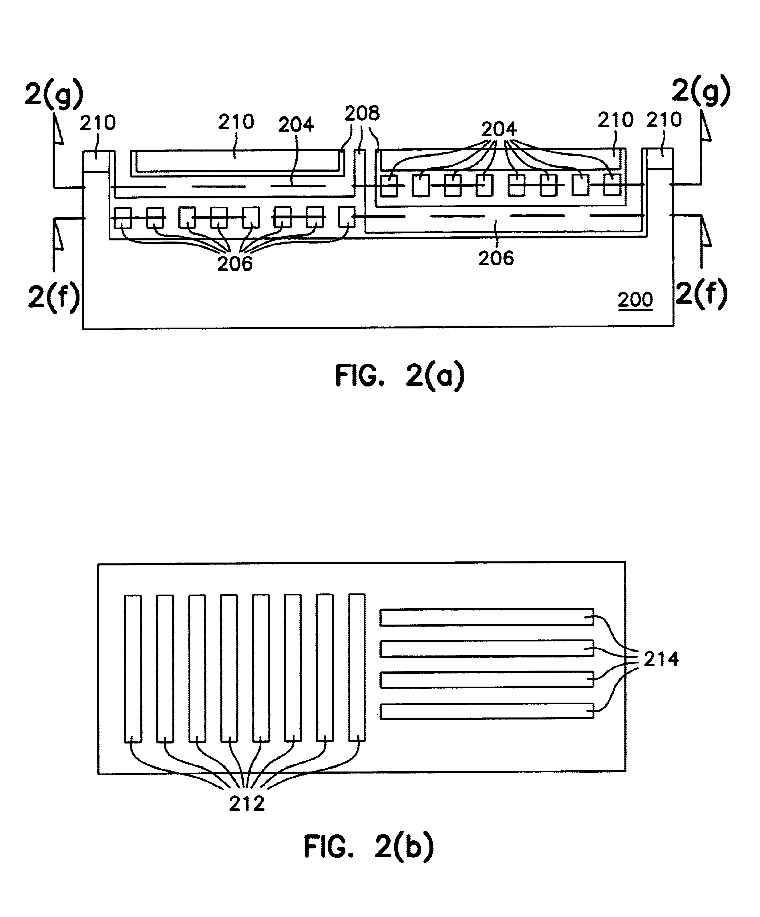
[0015]In the following detailed description of exemplary embodiments of the invention, reference is made to the accompanying drawings which form a part hereof, and in which is shown by way of illustration specific exemplary embodiments in which the invention may be practiced. These embodiments are described in sufficient detail to enable those skilled in the art to practice the invention, and it is to be understood that other embodiments may be utilized and that logical, mechanical, electrical and other changes may be made without departing from the spirit or scope of the present invention. The following detailed description is, therefore, not to be taken in a limiting sense, and the scope of the present invention is defined only by the appended claims.

[0016]The detailed description is divided into five sections. In the first section, exemplary structures having buried conductors are described. In the second section, a method by which buried conductors may be formed according to one...


PUM


Abstract

Buried conductors within semiconductor devices and structures, and methods for forming such conductors, are disclosed. In one embodiment of the invention, a semiconductor structure includes a substrate and a plurality of conductive elements buried within the substrate. The conductive elements may be metal, such as tungsten or a tungsten alloy. The invention described in the disclosure provides for advantages including formation of three-dimensional structures without resort to external wiring.

Description

[0001]This application is a division of Ser. No. 09 / 069,326 filed Apr. 29, 1998.RELATED APPLICATION[0002]This application is related to cofiled, and coassigned application entitled “Hi Q Inductive Elements”, Ser. No. 09 / 069,346, now U.S. Pat. No. 6,025,261.FIELD OF THE INVENTION[0003]This invention relates generally to semiconductor technology, and more particularly to buried conductors within semiconductor devices and structures, and methods for forming such conductors.BACKGROUND OF THE INVENTION[0004]Semiconductor technology pervades most electronic devices today. Computers, televisions, videocassette recorders, cameras, etc., all use semiconductor integrated circuits to varying degrees. For example, the typical computer includes microprocessors and dedicated controller integrated circuits (i.e., video controllers, audio controllers, etc.), as well as memory, such as dynamic random-access memory.[0005]Traditionally, the semiconductor industry has used a process that requires first...

Claims


Application Information

Patent Timeline
IPC IPC(8): H01L21/70H01L23/52H01L21/768H01L23/535
CPCH01L21/743H01L21/76898H01L23/535H01L2223/54453H01L2924/0002H01L2924/00
Inventor FARRAR, PAUL A.NOBLE, WENDELL P.
Owner MICRON TECH INC
Why Eureka
Try Eureka