
Programmable data strobe offset with DLL for double data rate (DDR) RAM memory

Inactive Publication Date: 2005-09-06
AGERE SYST INC
View PDF28 Cites 127 Cited by
  • Summary
  • Abstract
  • Description
  • Claims
  • Application Information

AI Technical Summary

Benefits of technology

"The present invention provides a method for optimizing memory access strobes by using a delay locked loop (DLL) circuit to delay the data access signal to a center of a data window and adjusting the initial delay through a fine tuning offset determined by a memory test. Additionally, a DQS strobe controller for a double data rate (DDR) memory device is provided that includes a delay line and an adder / subtracter element to implement the fine tuning adjustment of the initial delay. The technical effects of this invention include improved memory access speed and reliability."

Problems solved by technology

To achieve the ideal 90° phase shift, one of the most difficult issues addressed in the design of a Double Data Rate (DDR) SDRAM controller is delaying the SDRAM data strobe (DQS) to the center of the read window.
In particular, this delay is usually based on a calculated optimal value, which may not, in practice, be the optimal value.
One of the disadvantages of such a conventional SDRAM controller is that it relies on dividing a clock period by a value, n, to obtain a desired delay.

Method used


Image

  • Programmable data strobe offset with DLL for double data rate (DDR) RAM memory
  • Programmable data strobe offset with DLL for double data rate (DDR) RAM memory
  • Programmable data strobe offset with DLL for double data rate (DDR) RAM memory

Examples


Embodiment Construction

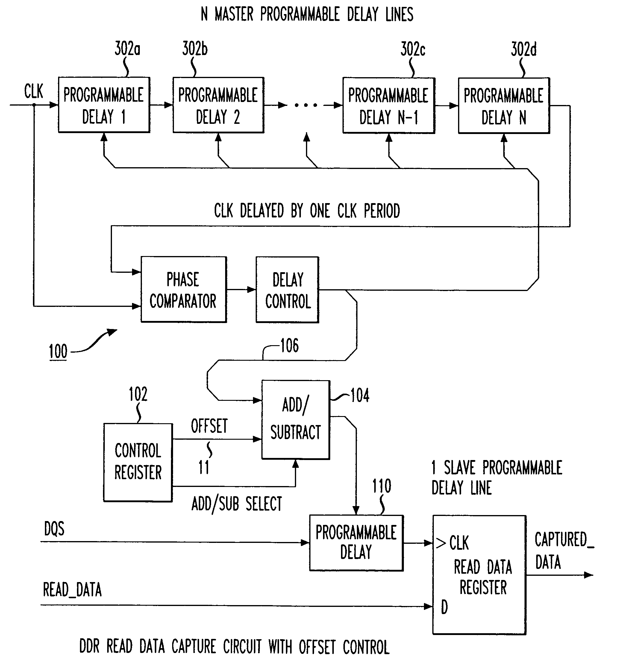
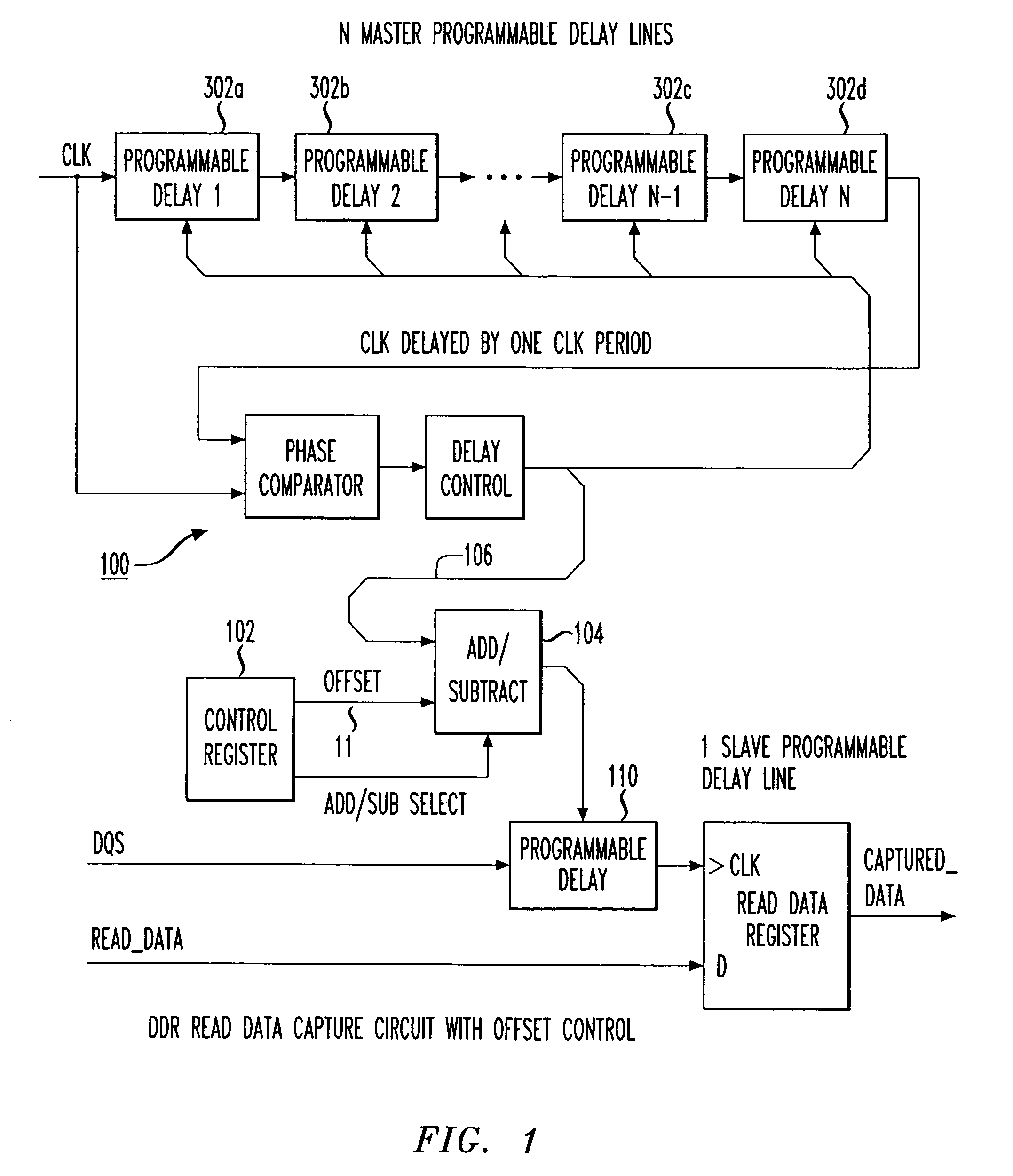
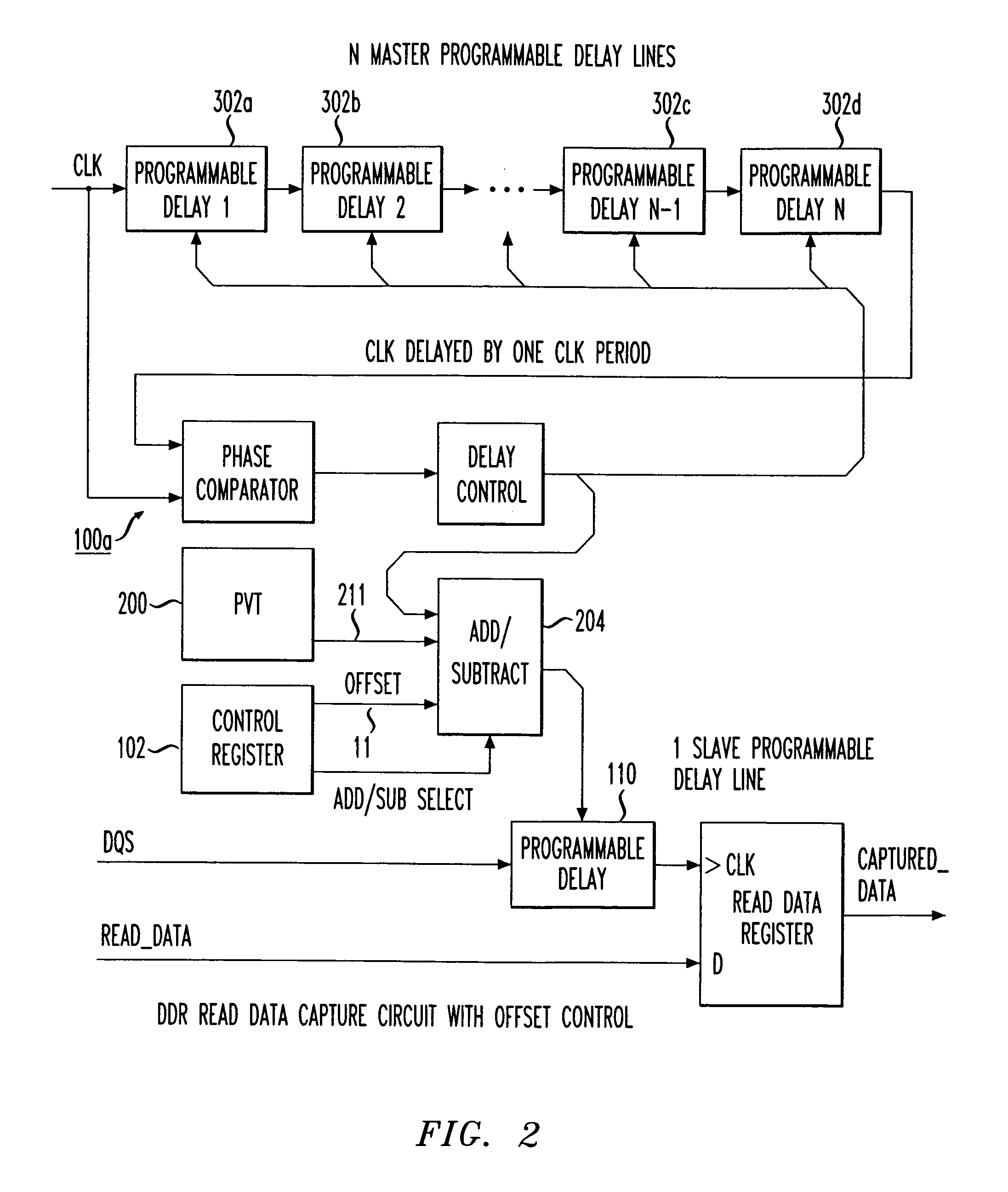
[0022]Conventional DQS data strobes are centered based on fixed, predetermined designs. The present invention improves upon conventional DQS data strobes by providing a technique for tweaking the DQS data strobe delay resulting in a more exact, actual center of a received data eye. In an additional embodiment, the present invention also adds compensation for actual on-chip delay changes due to voltage and / or temperature fluctuations.

[0023]Thus, the present invention provides a DDR SDRAM controller that determines and locks-in on the actual center of the DDR SDRAM received (read) data window, or “eye”. While disclosed with respect to a DDR-DRAM in particular, the invention relates as well to DDR-RAM in general, or even to any memory controller that captures data from a source that also provides the capture clock or strobe.

[0024]Accordingly, the present invention provides better centering of DQS data strobes by integrating a fine adjustment, or “tweaking”, of a DQS delay via a program...


PUM


Abstract

A double data rate (DDR) synchronous dynamic RAM (SDRAM), or DDR-SDRAM, memory controller employing a delay locked loop (DLL) circuit to delay an SDRAM data strobe (DQS) signal to the center, or ‘eye’ of the read data window. However, in distinction from conventional techniques, the initial delay determined by the DLL is fine tuned with an offset determined by a memory test. Moreover, in an additional embodiment, the delay may be further adjusted during operation to compensate for environmental conditions by a PVT (process, value, temperature) circuit.

Description

BACKGROUND OF THE INVENTION[0001]1. Field of the Invention[0002]This invention relates to semiconductor circuits. More particularly, it relates to circuitry used to access data in a memory device.[0003]2. Background of Related Art[0004]The basic principle of Double Data Rate (DDR) Synchronous Dynamic Random Access Memory (SDRAM), or DDR-SDRAM, is very simple. DDR-SDRAM is RAM that transfers data on both 0-1 and 1-0 clock transitions, theoretically yielding twice the data transfer rate of normal SDRAM. Thus, while a DDR-SDRAM memory module is clocked at the same speed as normal SDRAM, it is able to transport double the amount of data by using the rising as well as falling edge of the clock signal for data transfers.[0005]During any data access, a controller provides the DDR SDRAM with a clock, inverted clock, address, and control signals. During a write cycle, the controller also provides data as well as a data strobe signal (DQS). During a read cycle, the DDR-SDRAM provides data and...

Claims


Application Information

Patent Timeline
Patent Type & Authority Patents(United States)
IPC IPC(8): G11C7/00G11C7/10
CPCG11C7/1078G11C7/1093G11C7/222
Inventor DAHLBERG, JAMES A.DUARDO, OBED
Owner AGERE SYST INC
Learn More