
Apparatus and method for electrolytically depositing copper on a semiconductor workpiece

a technology of electrolytic depositing and workpiece, which is applied in the direction of electrolysis components, printed circuit manufacturing, printed element electric connection formation, etc., can solve the problems of limiting the performance of integrated circuits, reducing the speed at which the integrated circuit may process electrical signals, and propagation delays, so as to achieve enhanced seed layers and ultra-thin seed layers.

Inactive Publication Date: 2005-08-23
SEMITOOL INC
View PDF61 Cites 197 Cited by
  • Summary
  • Abstract
  • Description
  • Claims
  • Application Information

AI Technical Summary

Problems solved by technology

Delays in propagation of electrical signals between devices on a single die limit the performance of integrated circuits.
More particularly, these delays limit the speed at which an integrated circuit may process these electrical signals.
Larger propagation delays reduce the speed at which the integrated circuit may process the electrical signals, while smaller propagation delays increase this speed.
Despite the advantageous properties of copper, it has not been as widely used as an interconnect material as one would expect.
This is due, at least in part, to the difficulty of depositing copper metallization and, further, due to the need for the presence of barrier layer materials.
A CVD process can result in conformal copper coverage over a variety of topological profiles, but such processes are expensive when used to implement an entire metallization layer.
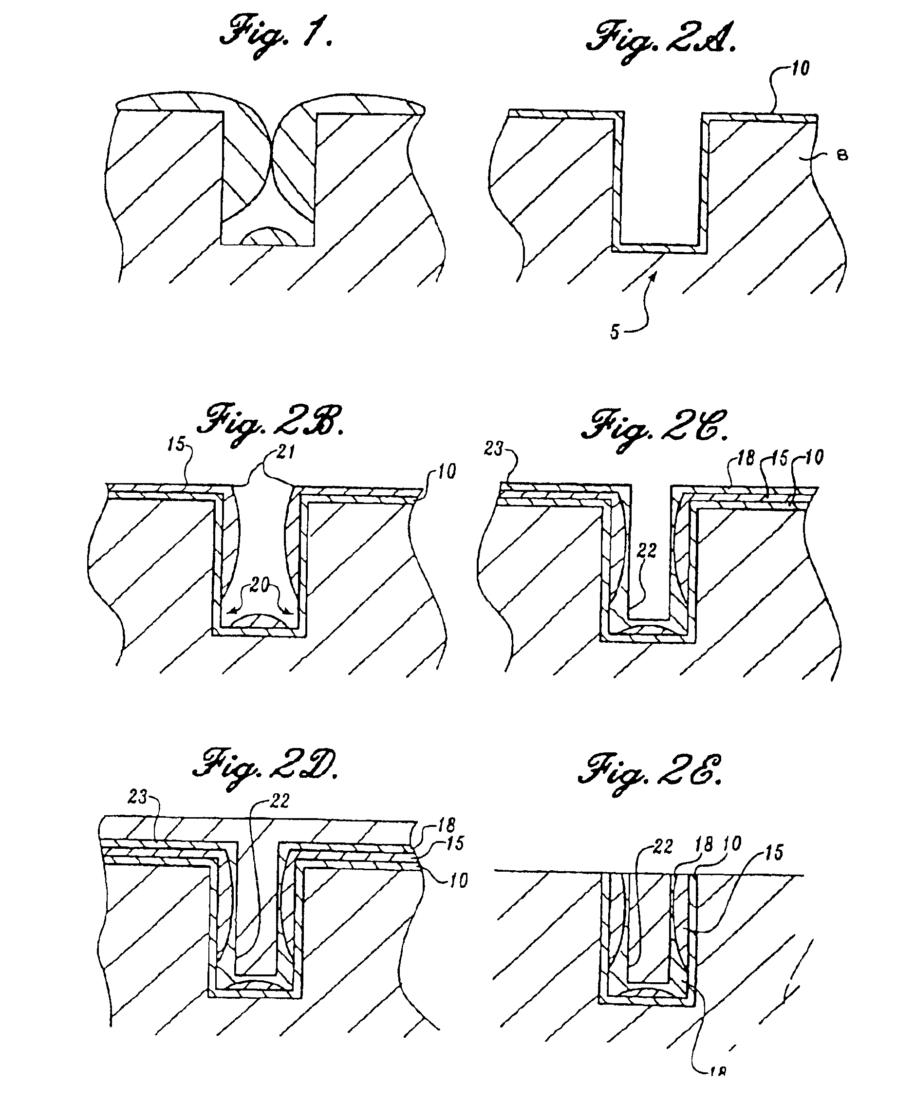
One disadvantage of PVD processes, however, is that they result in poor (non-conformal) step coverage when used to fill microstructures, such as vias and trenches, disposed in the surface of the semiconductor workpiece.
This result in an open void region that seriously impacts the ability of the metallization line to carry the electrical signals for which it was designed.
These techniques, however, are generally only suitable for applying copper to an electrically conductive layer.
Techniques for electrodeposition of copper on a barrier layer material have not heretofore been commercially viable.

Method used


Image

  • Apparatus and method for electrolytically depositing copper on a semiconductor workpiece
  • Apparatus and method for electrolytically depositing copper on a semiconductor workpiece
  • Apparatus and method for electrolytically depositing copper on a semiconductor workpiece

Examples


example 1

Comparison of Acid Copper Plating With and Without Seed Layer Enhancement

[0041]Semiconductor wafers 1, 2 and 3 were each coated with a 200 Angstrom PVD copper seed layer. In accordance with the present invention, wafers 1 and 2 had seed layer enhancement from citric acid and EDTA baths, respectively, the compositions of which are set forth below:[0042]Bath for Wafer 1: 0.1 M Cu SO4+0.2 M Citric acid+0.05 M H3BO3 in D.I. water at pH 9.5, temperature 25° C.[0043]Bath for Wafer 2: 0.1 M Cu SO4+0.2 M EDTA acid+0.05M H3BO3 in D.I. water at pH 12.5, temperature 25° C.

Wafer 3 did not have any seed layer enhancement.

[0044]The three wafers were then plated with a 1.5 micron copper layer from an acid copper bath under identical conditions. The following Table compares the uniformities, as deduced from sheet resistance measurements, of the three wafers after the deposition of a copper layer having a nominal thickness of 1.5 microns.

[0045]

TABLE 1Non-UniformityStandardEnhancementDeviationWaferBa...


PUM

PropertyMeasurementUnit
diameteraaaaaaaaaa
thicknessaaaaaaaaaa
thicknessaaaaaaaaaa

Abstract

A process for applying a metallization interconnect as to a semiconductor workpiece having a barrier layer deposited on a surface thereof is set forth. The process includes the forming of an ultra-thin metal seed layer on the barrier layer. The ultra-thin seed layer having a thickness of less than or equal to about 500 Angstroms. The ultra-thin seed layer is then enhanced by depositing additional metal thereon to provide an enhanced sed layer. The enhanced seed layer has a thickness at all points on sidewalls of substantially all recessed features distributed within the workpiece that is equal to or greater than about 10% of the nominal seed layer thickness over an exteriorly disposed surface of the workpiece.

Description

CROSS-REFERENCE TO RELATED APPLICATION(S)[0001]This application is a continuation of U.S. application Ser. No. 10 / 302,711, filed Nov. 22, 2002 now U.S. Pat. No. 6,638,410 which is a continuation of U.S. patent application Ser. No. 09 / 694,413 filed Oct. 23, 2000, now U.S. Pat. No. 6,632,345, which is a continuation of U.S. patent application Ser. No. 09 / 045,245, filed Mar. 20, 1998, now U.S. Pat. No. 6,197,181.BACKGROUND OF THE INVENTION[0002]An integrated circuit is an interconnected ensemble of devices formed within a semiconductor material and within a dielectric material that overlies a surface of the semiconductor. Devices which may be formed within the semiconductor include MOS transistors, bipolar transistors, diodes and diffused resistors. Devices which may be formed within the dielectric include thin-film resistors and capacitors. Typically, more than 100 integrated circuit die (IC chips) are constructed on a single 8 inch diameter silicon wafer. The devices utilized in each...

Claims


Application Information

Patent Timeline
Patent Type & Authority Patents(United States)
IPC IPC(8): H01L21/02H01L21/70H01L21/288H01L21/768H05K3/42
CPCH01L21/2885H01L21/76843H01L21/76868H01L21/76873H01L2221/1089H05K3/423
Inventor CHEN, LINLINTAYLOR, THOMAS
Owner SEMITOOL INC
Learn More