
Display module

a display module and active matrix technology, applied in the field of active matrix display modules, can solve the problems of deteriorating power efficiency and large power consumption loss, and achieve the effects of improving the aperture ratio of pixels, preventing such display faults as line defects, and high quality

Inactive Publication Date: 2005-07-19
SAMSUNG DISPLAY CO LTD +1
View PDF8 Cites 44 Cited by
  • Summary
  • Abstract
  • Description
  • Claims
  • Application Information

AI Technical Summary

Benefits of technology

[0025]The present invention is to provide a display module incorporating such an electrooptic device as the OLED therein, the arrangement of which module allows the aperture ratio of the pixels to improve and to prevent such display fault as line defect so as to display image with high quality as well as avoids the increase of the number of production process thereof.
[0027]This arrangement allows the aperture ratio of the pixels to improve and image to be displayed with high quality as well as avoids the increase of the number of the production steps thereof so as to reduce the production cost. The more concrete arrangements of the display module according to the present invention are described below.

Problems solved by technology

Thus, it is unavoidable that the driving voltage and current in use enlarge, which causes large loss of power consumption such as heating so as to deteriorate power efficiency.

Method used


Image

  • Display module
  • Display module
  • Display module

Examples


Embodiment Construction

[0045]Hereinafter, the preferred embodiments of the present invention are described in details with reference to the accompanying drawings. The organic emitting layer of the respective pixels as described below is divided into such types as emitting light with luminance in proportion to the value of the current and with a color (including white) inherent in an organic material in use and incorporating a red, green, blue or other color filter into the organic layer to emit white light so as to display color image.

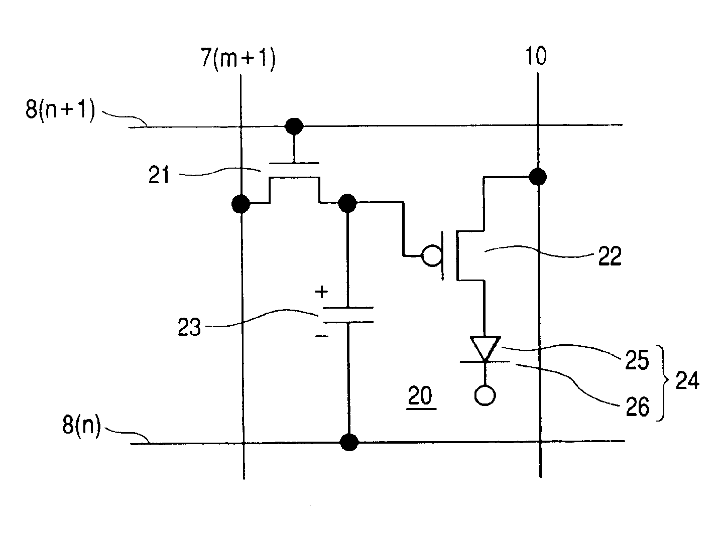
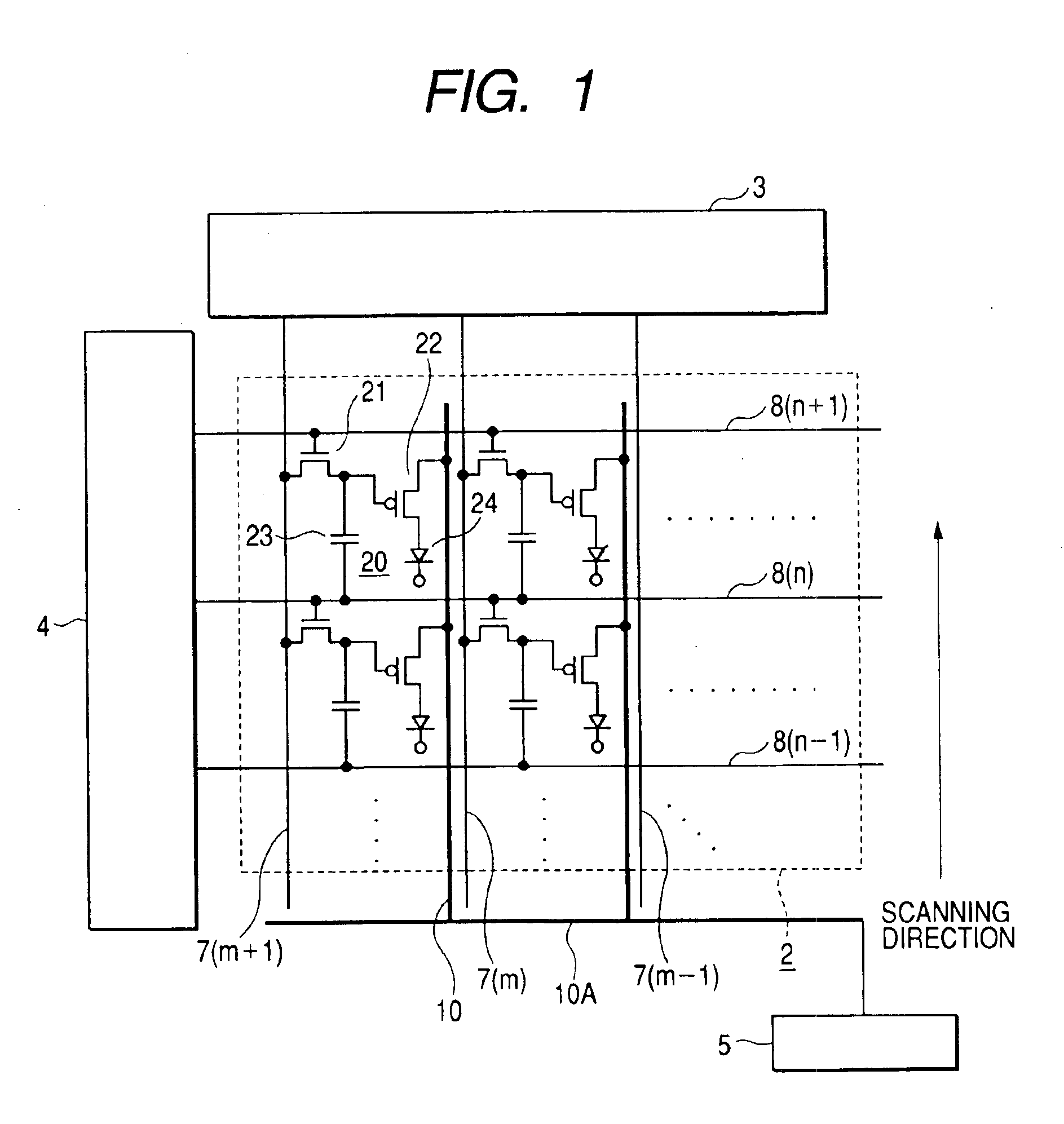
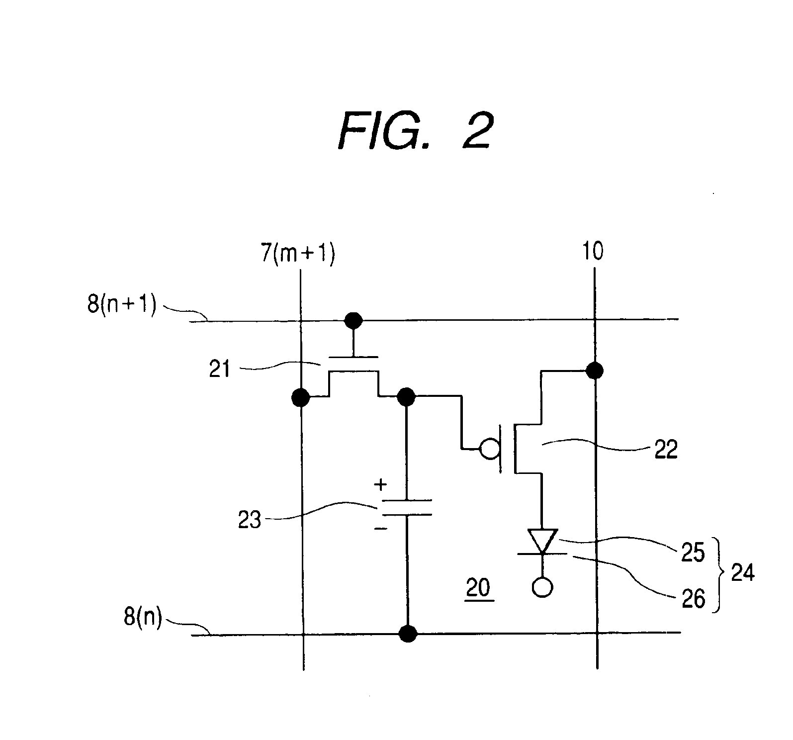
[0046]FIG. 1 is a block diagram to show the arrangement of the first embodiment of the display module according to the present invention while FIG. 2 is a circuit view to show the detailed arrangement of one pixel of the module as shown in FIG. 1. In the present embodiment, in the same way as shown in FIG. 10, data lines 7, scanning lines 8 and current supply lines 10 are provided in the display region 2. In the drawings, the scanning lines 8 are represented with 8(n+1), 8(n...


PUM


Abstract

An organic light emitting diode (OLED) display module is provided wherein the aperture ratio of the respective pixels thereof improves and such display faults as line defect is prevented so as to allow image to be displayed with high quality. The display module is provided with a capacitor, a first terminal of which is connected to an output terminal of the first transistor as selected by the scanning line and a second terminal of which is connected to the gate placed anterior thereto, wherein the electric current is supplied to an organic emitting device in response to the data signal as supplied from the data line through the second transistor, which turns into on-state condition when the first transistor is put into an off-state condition, and as stored in the capacitor.

Description

FIELD OF THE INVENTION[0001]The present invention relates to an active matrix display module, especially, pertaining to such display module as being provided with pixels comprising such emitting devices as an EL (electro luminescence) device or a LED (light emitting diode) wherein light is emitted by conducting electric current through such an emitting layer as an organic semiconductor thin film and with pixels circuits to control the emitting operation of those pixels.BACKGROUND OF THE INVENTION[0002]Recently, the advent of advanced information network system in our modern life increases the demand for personal computers, car navigation systems, portable remote terminals and communication network equipment or the combined products thereof. For such products as mentioned above, such a display device as being thin in thickness, light in weight and of lower power consumption is suitable so that a liquid crystal display or a display module incorporating such electrooptic devices as a s...

Claims


Application Information

Patent Timeline
IPC IPC(8): G09G3/32G09F9/30G09G3/20G09G3/30H01L27/32H01L51/50
CPCG09G3/3233G09G3/3241G09G2300/0465G09G2300/0842G09G2300/0876G09G2310/0262G09G3/30H10K59/131H10K59/123H10K59/1216
Inventor SATO, TOSHIHIROKANEKO, YOSHIYUKIMIKAMI, YOSHIROOUCHI, TAKAYUKI
Owner SAMSUNG DISPLAY CO LTD
Learn More