Circuit and method for transforming data input/output format in parallel bit test

a data input/output format and data input/output technology, applied in the field of semiconductor memory devices, can solve problems such as the inability to check failures between two adjacent input/output lines

Inactive Publication Date: 2005-06-21
SAMSUNG ELECTRONICS CO LTD
View PDF3 Cites 11 Cited by
  • Summary
  • Abstract
  • Description
  • Claims
  • Application Information

AI Technical Summary

Benefits of technology

The present invention provides a circuit and method for transforming the data input / output format of a semiconductor memory device. This circuit can generate various data patterns when the number of memory cells connected to one column selection line is greater than the number of data input pins. The circuit includes a first transmission circuit and a second transmission circuit that can activate at different times and transmit data to different memory cells. The circuit also includes a command register that can output signals to activate the first and second transmission circuits based on external commands and addresses. The technical effect of this invention is to improve the flexibility and efficiency of data transmission in a semiconductor memory device.

Problems solved by technology

However, when data patterns of Table 1 are used, it is impossible to check failures between two adjacent input / output lines, e.g., between an input / output line connected to the memory cell MC0 and an input / output line connected to the memory cell MC1 or between an input / output line connected to the memory cell MC4 and an input / output line connected to the memory cell MC5.

Method used


Image

  • Circuit and method for transforming data input/output format in parallel bit test
  • Circuit and method for transforming data input/output format in parallel bit test
  • Circuit and method for transforming data input/output format in parallel bit test

Examples


Embodiment Construction

[0024]The present invention now will be described more fully with reference to the accompanying drawings, in which preferred embodiments of the invention are shown.

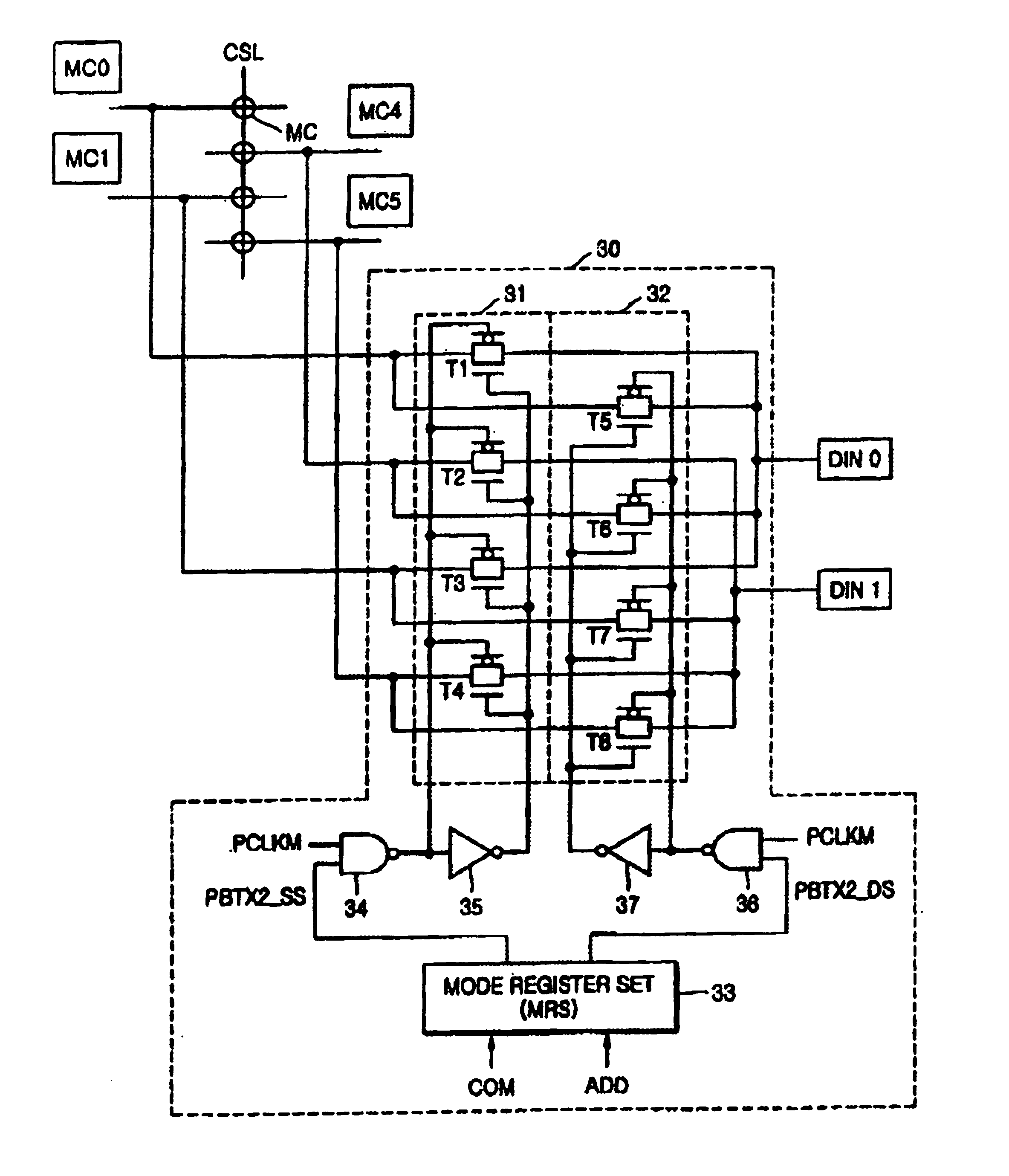
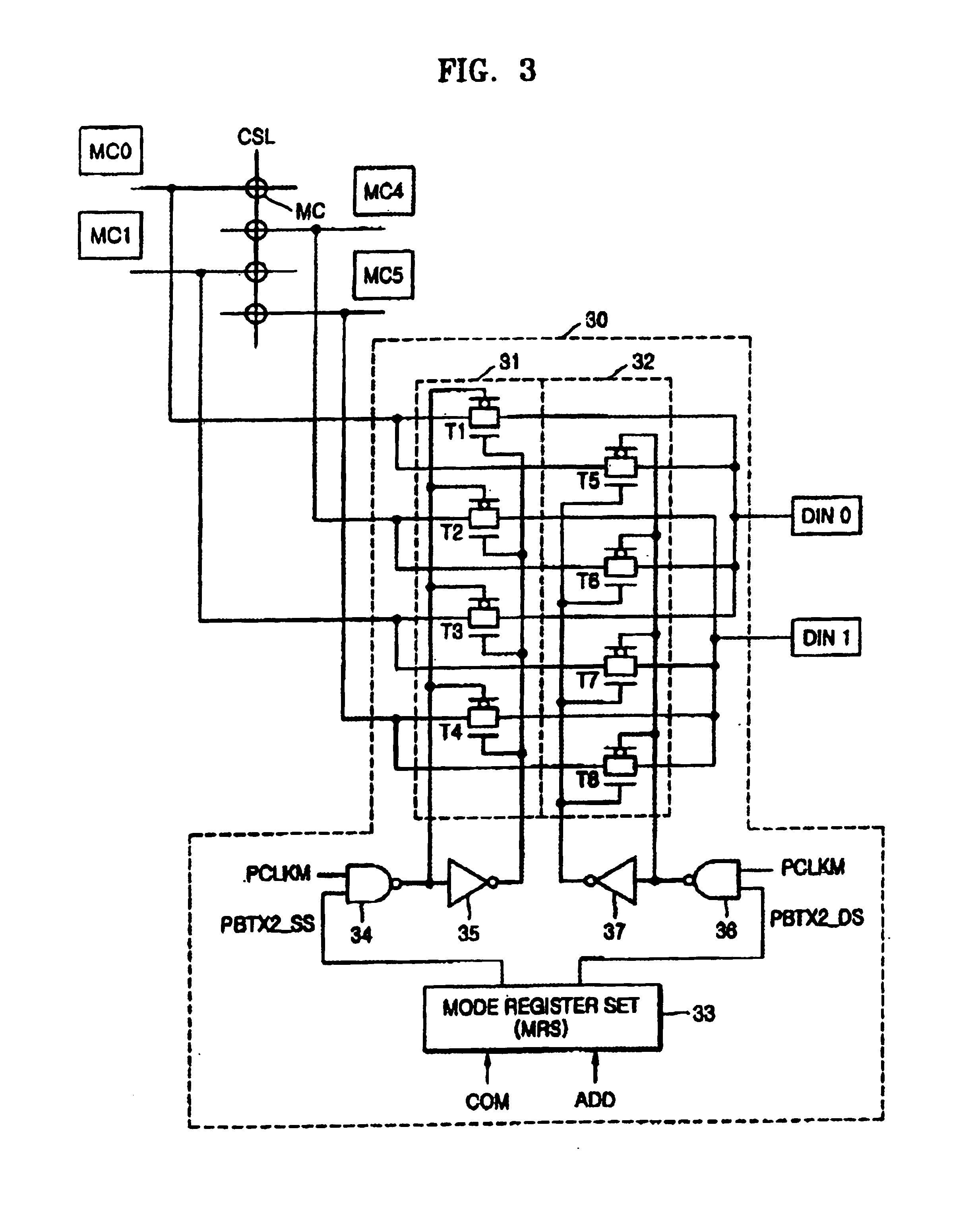
[0025]FIG. 3 is a view of a circuit for transforming data input / output format according to an embodiment of the present invention.

[0026]Referring to FIG. 3, a circuit 30 for transforming a data input / output format according to an embodiment of the present invention includes a first transmission circuit 31, a second transmission circuit 32, a mode register set (MRS) 33, NAND gates 34 and 36, and inverters 35 and 37.

[0027]The first transmission circuit 31 is activated when a first test mode signal PBTX2_SS is enabled as logic high, receives two data inputs from two data input ends DIN0 and DIN1, and transmits the data inputs to four memory cells (MC) MC0, MC1, MC4, and MC5. The second transmission circuit 32 is activated when a second test mode signal PBTX2_DS is enabled as logic high, receives two data inputs from two data...


PUM


Abstract

Provided are a circuit and a method for transforming a data input / output format of a semiconductor memory device which is capable of generating various types of data patterns when the number of memory cells connected to one column selection line is greater than the number of data input pins. The circuit for transforming a data input / output format of a semiconductor memory device includes a first transmission circuit, a second transmission circuit, and a mode register set (MRS). The first transmission circuit is activated when a first test mode signal is enabled, receives n data inputs from n data input ends, and transmits the n data inputs to m memory cells. Here, n and m are natural numbers and m is greater than n. The second transmission circuit is activated when a second test mode signal is enabled, receives n data inputs from the n data input ends, and transmits the n data inputs to the m memory cells. The mode register set (MRS) receives a command and an address from outside the semiconductor device and outputs the first test mode signal and the second test mode signal according to combinations of the command and the address. In particular, data that is transmitted to adjacent memory cells of the m memory cells is inputted to different input ends of the n data input ends.

Description

[0001]This application claims priority from Korean Patent Application No. 2002-72477, filed on Nov. 20, 2002, in the Korean Intellectual Property Office, the contents of which are incorporated herein in their entirety by reference.BACKGROUND OF THE INVENTION[0002]1. Field of the Invention[0003]The present invention relates to a semiconductor memory device, and more particularly, to a circuit and a method for transforming a data input / output format in a parallel bit test (PBT).[0004]2. Description of the Related Art[0005]A parallel bit test (PBT) is used to check failures of memory cells and write / read paths by writing and reading data to and from the memory cells of a semiconductor memory device in parallel. If the number of data input / output pins (DQ) is reduced in the parallel bit test (PBT), more memory devices can be tested at the same time. For example, if 16 monitoring pins can be used in test equipment, two X8 mode memory devices, four X4 mode memory devices, or eight X2 mode...

Claims


Application Information

Patent Timeline
Patent Type & Authority Patents(United States)
IPC IPC(8): G11C29/48G11C29/04G11C29/00
CPCG11C29/1201G11C29/48G11C2029/2602G11C29/00
Inventor RYU, JIN-HOSHIN, CHOONG-SUNCHU, YONG-GYU
Owner SAMSUNG ELECTRONICS CO LTD
Why Eureka
Try Eureka