Semiconductor device
a semiconductor and device technology, applied in the direction of transistors, digital storage, instruments, etc., can solve the problems of difficult to influence the luminance of the dispersed transistor characteristics, the same size, and the electric current flow,
- Summary
- Abstract
- Description
- Claims
- Application Information
AI Technical Summary
Benefits of technology
Problems solved by technology
Method used
Image

Examples
embodiment mode 1
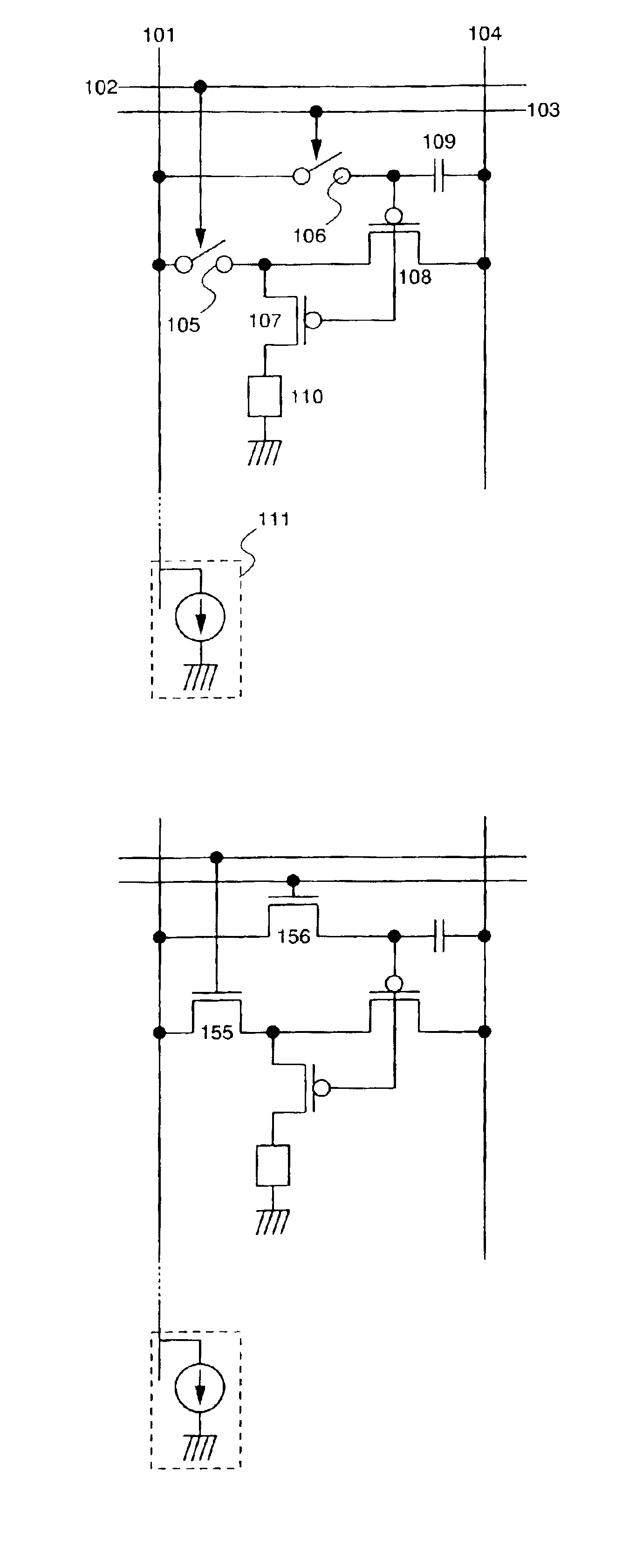
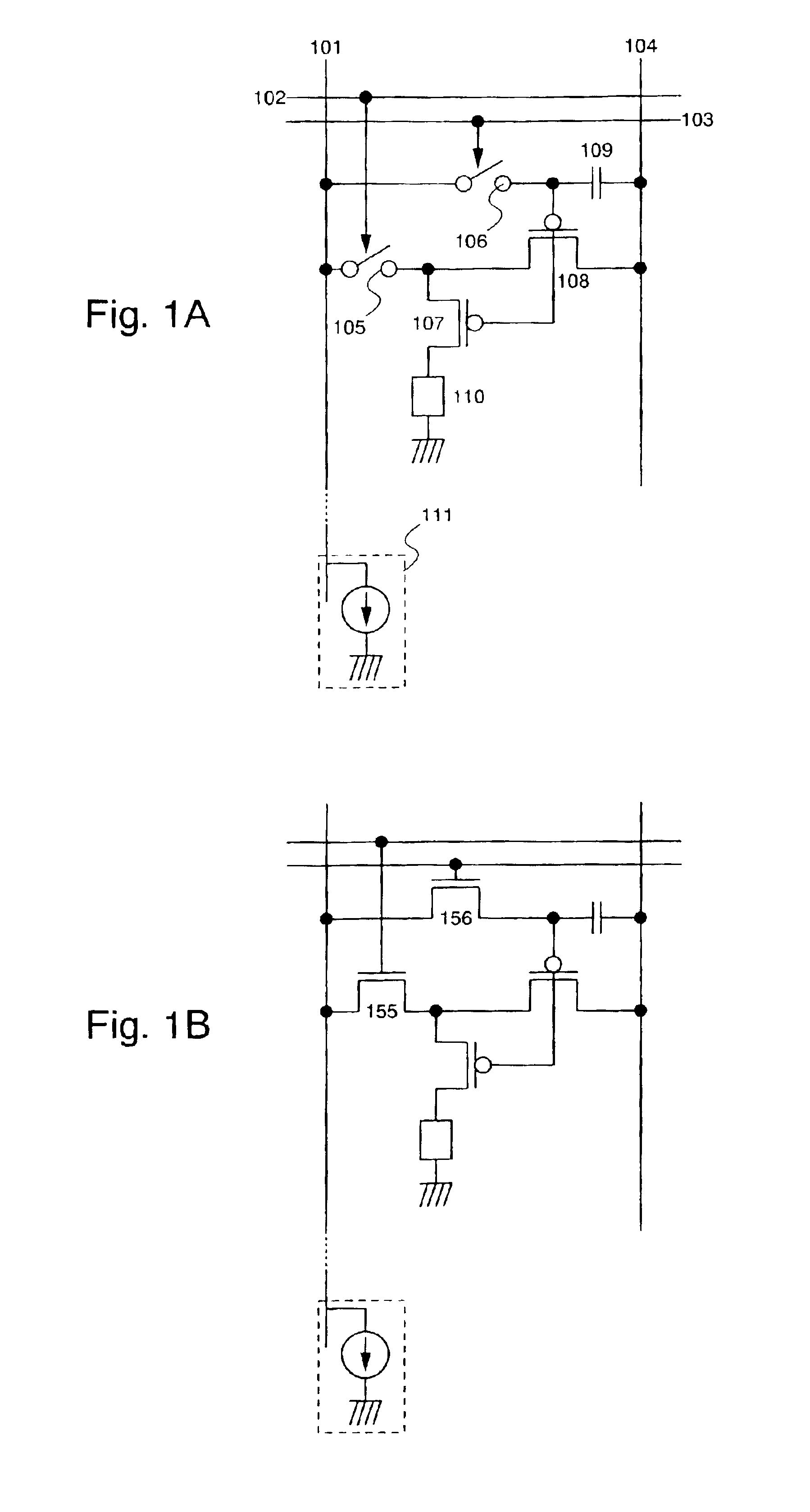
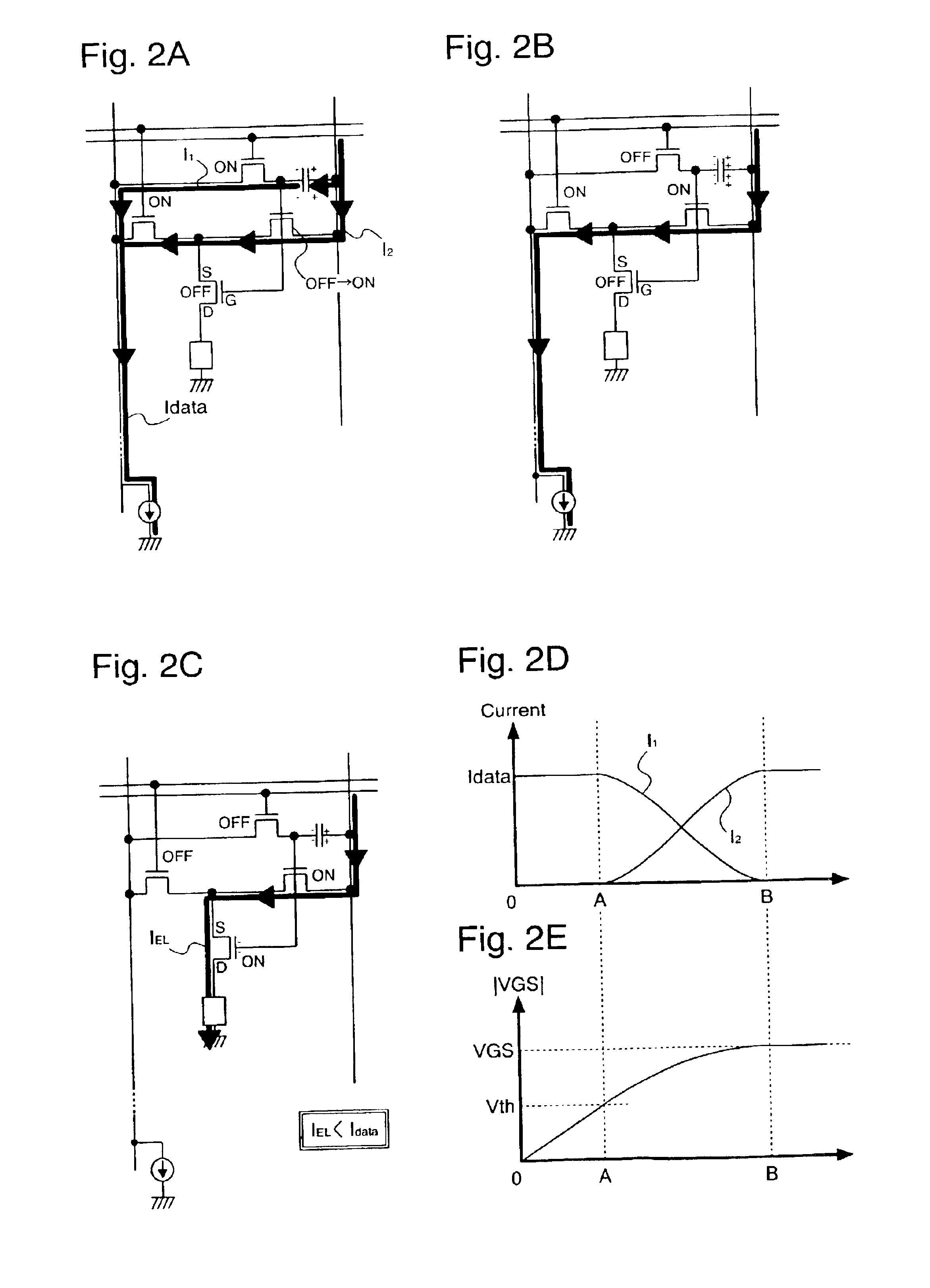
[0174]A structure of the present invention is shown in FIG. 1A. A pixel of FIG. 1A has a source signal line 101, first and second gate signal lines 102 and 103, an electric current supply line 104, a first switching element 105, a second switching element 106, a driver TFT 107, a converter and driver TFT 108, a storage capacitor 109, an EL element 110, and a current source for inputting signal electric current 111.
[0175]Note that the storage capacitor 109 may be formed as a capacitive element by using wirings, active layers, gate materials, and the like, with an insulating layer in between, and may also be eliminated by using a transistor gate capacitor instead. That is, provided that it has the capability to store the voltage between a gate and a source of the converter and driver TFT 108 for a required period of time, any structure may be used.
[0176]The first switching element 105 is controlled by the first gate signal line 102. A first electrode of the first switching element 105...
embodiment mode 2
[0196]Embodiment Mode 2 of the present invention is shown in FIG. 28A. A pixel of FIG. 28A has a source signal line 2801, first and second gate signal lines 2802 and 2803, an electric current supply line 2804, a first switching element 2805, a second switching element 2806, a driver TFT 2807, a converter and driver TFT 2808, a storage capacitor 2809, and an EL element 2810. Each source signal line has a current source for inputting signal electric current 2811.
[0197]Note that the storage capacitor 2809 may be formed as a capacitive element by using wirings, active layers, gate materials, and the like, with an insulating layer in between, and may also be eliminated by using a transistor gate capacitor instead. That is, provided that it has the capability to store the voltage between a gate and a source of the converter and driver TFT 2808 for a required period of time, any structure may be used.
[0198]The first switching element 2805 is controlled by the first gate signal line 2802. A...
embodiment 1
[0220]The structure of a semiconductor device for performing display using an analog image signal for an image signal is explained in Embodiment 1. An example of the structure of the semiconductor device is shown in FIG. 3A. There is a pixel portion 302, in which a plurality of pixels is arranged in a matrix shape, on a substrate 301. A source signal line driver circuit 303, and first and second gate signal line driver circuits 304 and 305 are in the periphery of the pixel portion 302. Although two gate signal line driver circuits are used in FIG. 3A, only one thereof need be used for cases in which it is not necessary to select a plurality of gate signal lines for pixel drive, as explained in the embodiment modes. Further, a structure in which the gate signal line driver circuits are disposed symmetrically at both ends of gate signal lines, and the gate signal lines are driven from both ends may also be used.
[0221]Signals input to the source signal line driver circuit 303, the firs...
PUM
 Abstract
Description
Claims
Application Information
 - R&D
- Intellectual Property
- Life Sciences
- Materials
- Tech Scout
- Unparalleled Data Quality
- Higher Quality Content
- 60% Fewer Hallucinations
Browse by: Latest US Patents, China's latest patents, Technical Efficacy Thesaurus, Application Domain, Technology Topic, Popular Technical Reports.
© 2025 PatSnap. All rights reserved.Legal|Privacy policy|Modern Slavery Act Transparency Statement|Sitemap|About US| Contact US: help@patsnap.com