Lead frame and semiconductor device using the lead frame and method of manufacturing the same

Inactive Publication Date: 2005-06-21
RENESAS ELECTRONICS CORP
View PDF16 Cites 8 Cited by
  • Summary
  • Abstract
  • Description
  • Claims
  • Application Information

AI Technical Summary

Benefits of technology

[0012]It is an object of the present invention to provide a technique which is capable of preventing a short-circuit or wire running condition in a semiconductor device having multi-leads from occurring and of stabilizing the bonding.
[0026]Furthermore, by mounting a semiconductor chip on a supporting body, the heat generated in the semiconductor chip can be radiated outside through the supporting body, thus making it possible to improve the heat radiation characteristics of the semiconductor chip.

Problems solved by technology

However, there is a problem in that a short-circuit in which adjacent wires come into contact with each other becomes more likely as the spacing becomes smaller when multi-leads and respective pad electrodes are bonded with each other using a wire of Au or the like.
Further, there is a problem in that wire running, in which a wire is transformed by the flow of molding resin due to the lowering of the mechanical strength of respective leads, or a decrease in the wire spacing sometimes occurs in the case of resin molding after wire bonding, and so a short-circuit of the wires is often produced under these circumstances.

Method used


Image

  • Lead frame and semiconductor device using the lead frame and method of manufacturing the same
  • Lead frame and semiconductor device using the lead frame and method of manufacturing the same
  • Lead frame and semiconductor device using the lead frame and method of manufacturing the same

Examples


Embodiment Construction

[0046]Embodiments of the present invention will be described hereinafter. In particular, in all of the drawings representing the various embodiments, identical reference numerals are assigned to those elements that have the same function, and repeated description thereof is omitted.

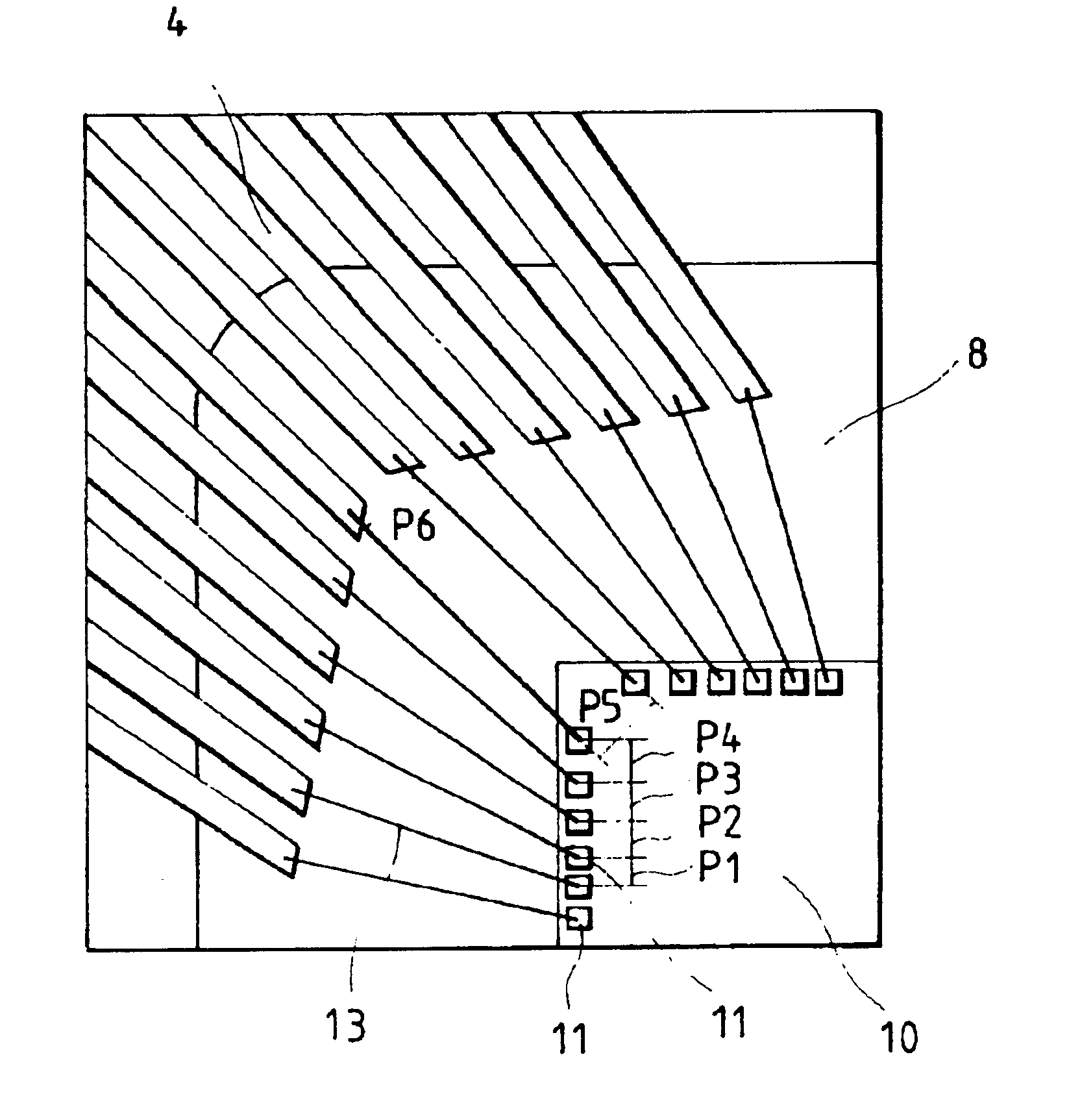
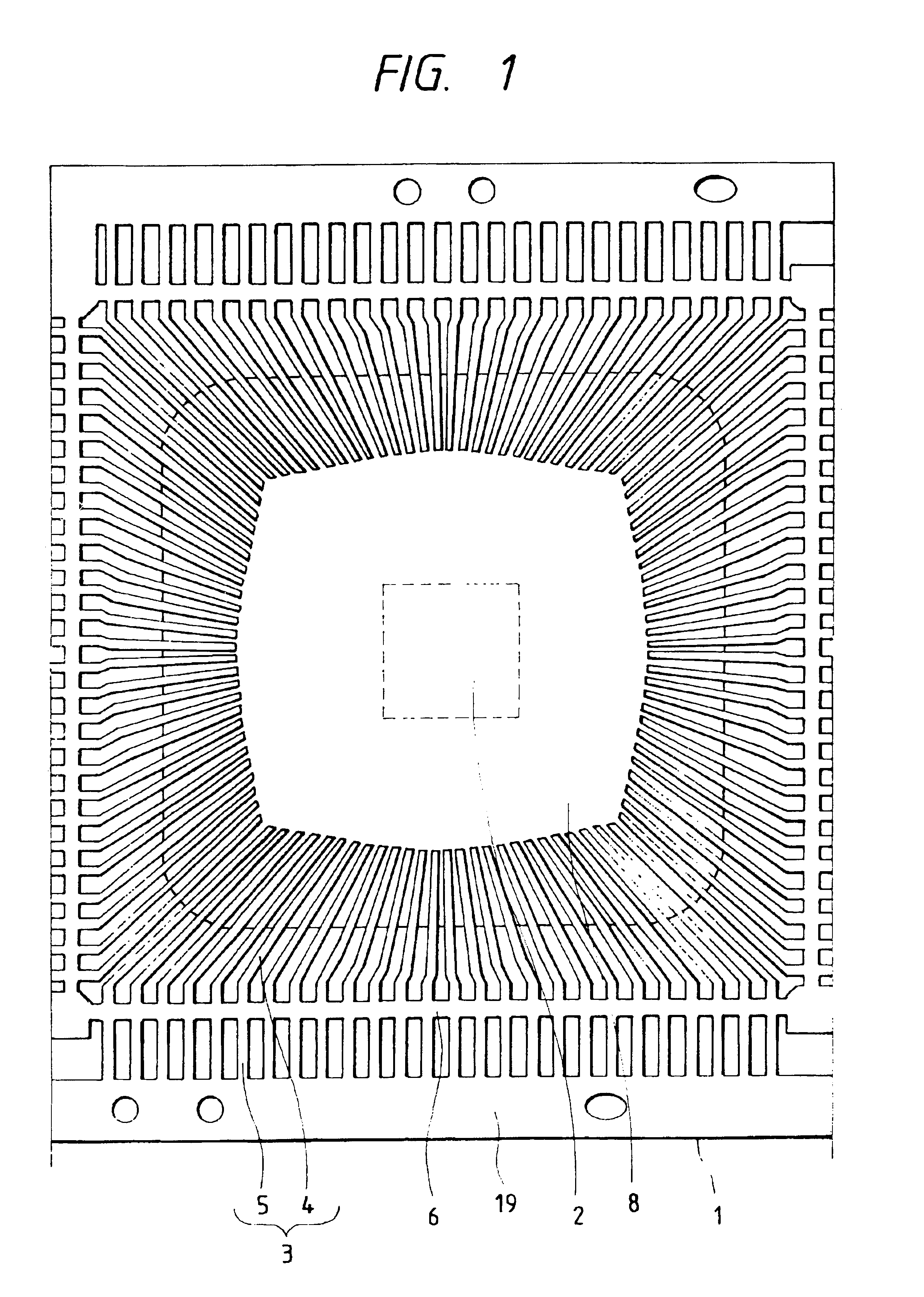
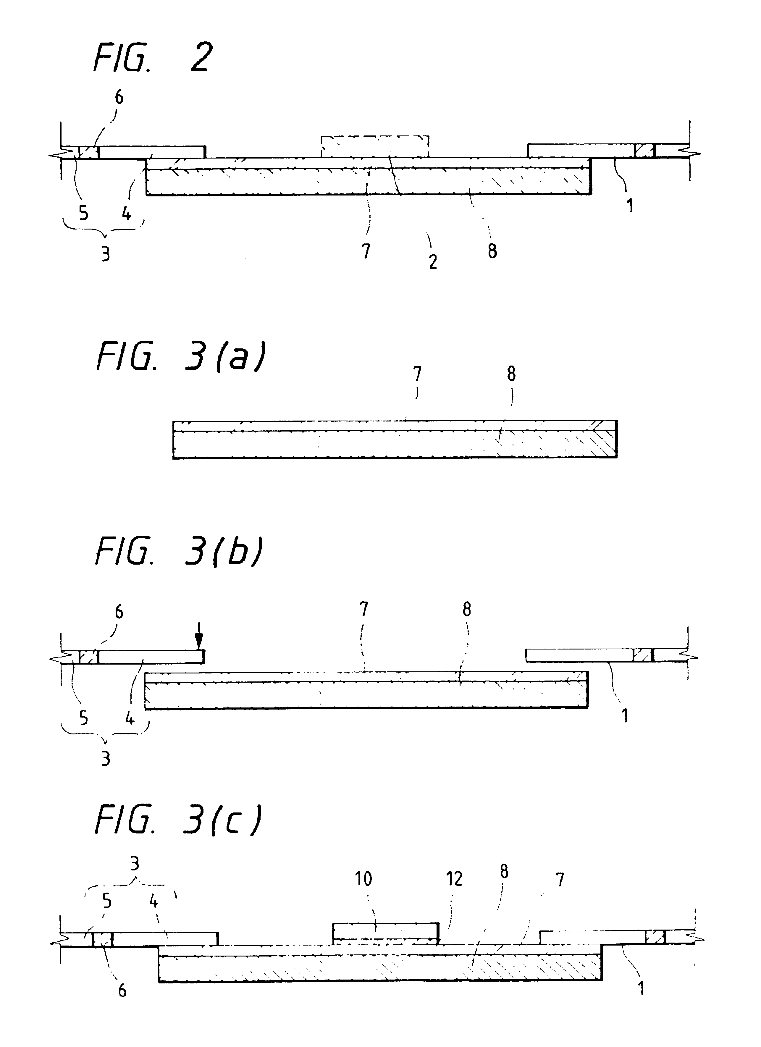
[0047]FIG. 1 is a plan view showing a lead frame used in a QFP type semiconductor device forming an embodiment of the present invention, and FIG. 2 is a longitudinal sectional view of the lead frame shown in FIG. 1. The lead frame 1 is made of a Fe—Ni alloy, for instance, and the points of the inner leads 4 of a plurality of leads 3 are arranged around the entire periphery of a semiconductor chip (shown with a broken line) mounting area 2 where a semiconductor chip is to be mounted at the center of the frame. Further, the lead frame 1 may be made of a Cu alloy.

[0048]Respective leads 3 are formed as one body with a dam bar 6 or a tie bar 19 to form a frame body of a lead frame and an inside portion and an ...


PUM


Abstract

A semiconductor device includes a substrate, a semiconductor chip mounted on one surface of the substrate, wherein the semiconductor chip has an integrated circuit and bonding pads formed on a main surface thereof. The main surface of the semiconductor chip has a quadrilateral shape with the bonding pads being disposed along four sides of the main surface. A plurality of conductors is disposed on the one surface of the substrate so as to surround the semiconductor chip along four sides thereof and a plurality of bonding wires electrically connect the bonding pads with tips of the conductors, respectively. A resin body seals the semiconductor chip, the conductors and the plurality of bonding wires. A pitch between adjacent bonding pads increases in a direction toward four corners defined by the four sides of the main surface of the semiconductor chip.

Description

CROSS REFERENCE TO RELATED APPLICATION[0001]This is a continuation of U.S. application Ser. No. 08 / 820,228, filed Mar. 18, 1997, now U.S. Pat. No. 6,265,762, the subject matter of which is incorporated by reference herein.BACKGROUND OF THE INVENTION[0002]The present invention relates to a lead frame and a semiconductor device, and more particularly to a technique which is applicable to a lead frame having multi-leads and a semiconductor device using the lead frame.[0003]In the production of a semiconductor device, such as an LSI, more complicated circuits are being fabricated and the number and type of functions are also increasing with improvement in the degree of integration. Because of the ability to provide increased functions, the semiconductor device has come to require more external terminals, and thus, the numbers of pad electrodes provided on a semiconductor chip and the number of leads that form the external terminals of a semiconductor device have increased in a correspon...

Claims


Application Information

Patent Timeline
IPC IPC(8): H01L23/495H01L23/433H01L23/34H01L23/48
CPCH01L23/4334H01L23/49541H01L24/06H01L24/49H01L24/85H01L2924/07802H01L2224/73265H01L2224/48647H01L2224/48624H01L2924/01033H01L2924/00014H01L24/48H01L2924/20753H01L2924/20752H01L2924/14H01L2924/01082H01L2924/01079H01L2924/01075H01L2924/01047H01L2924/01029H01L2924/01028H01L2924/01015H01L2924/01013H01L2924/01006H01L2924/01005H01L24/45H01L2224/05553H01L2224/05624H01L2224/05647H01L2224/45015H01L2224/45144H01L2224/48091H01L2224/48247H01L2224/49171H01L2224/85424H01L2224/85447H01L2224/92247H01L2224/78H01L2924/00H01L2924/181H01L2224/05554H01L2924/10162H01L2924/00012
Inventor TANAKA, SHIGEKIFUJISAWA, ATSUSHINAGANO, SOUICHIHIRANO, TSUGIHIKOOOTA, RYOUICHIKONNO, TAKAFUMITATEBE, KENICHIOKAMOTO, TOSHIAKI
Owner RENESAS ELECTRONICS CORP
Why Eureka
Try Eureka