
Circuit and method of multi-channel dual slope ADC with offset cancellation and hysteresis input

a dual-slope analog-to-digital converter and multi-channel technology, applied in analog/digital conversion, physical parameter compensation/prevention, instruments, etc., can solve the problem of residual charge on the external capacitor, data coupling error or channel coupling, and takes a substantial long initialization time. problem, to achieve the effect of reducing the cycle length

Active Publication Date: 2005-06-14
WINBOND ELECTRONICS CORP
View PDF3 Cites 11 Cited by
  • Summary
  • Abstract
  • Description
  • Claims
  • Application Information

AI Technical Summary

Benefits of technology

The present invention provides a multi-channel dual slope analog-to-digital converter (ADC) that reduces cycle length and chip area, and avoids coupling error between channels. The circuit includes an input circuit, integrator, comparator, control logic, and data counter. The offset cancellation logic and hysteresis logic are used to avoid residual voltage and unexpected problems. The residual voltage is retained at a constant value after measurement cycles begin. The technical effects of the present invention include reduced cycle length, reduced chip area, and improved accuracy of the conversion results.

Problems solved by technology

Whereas the drawbacks of this conventional scheme are: i. it takes substantially long time to initialize. ii. it requires a substantially large offset cancel capacitor, i.e. large chip area. iii. it has data coupling error or channel coupling er
Moreover, when initialization is not sufficiently long, a residual charge on the external capacitor can affect conversion result to following cycles.

Method used


Image

  • Circuit and method of multi-channel dual slope ADC with offset cancellation and hysteresis input
  • Circuit and method of multi-channel dual slope ADC with offset cancellation and hysteresis input
  • Circuit and method of multi-channel dual slope ADC with offset cancellation and hysteresis input

Examples


Embodiment Construction

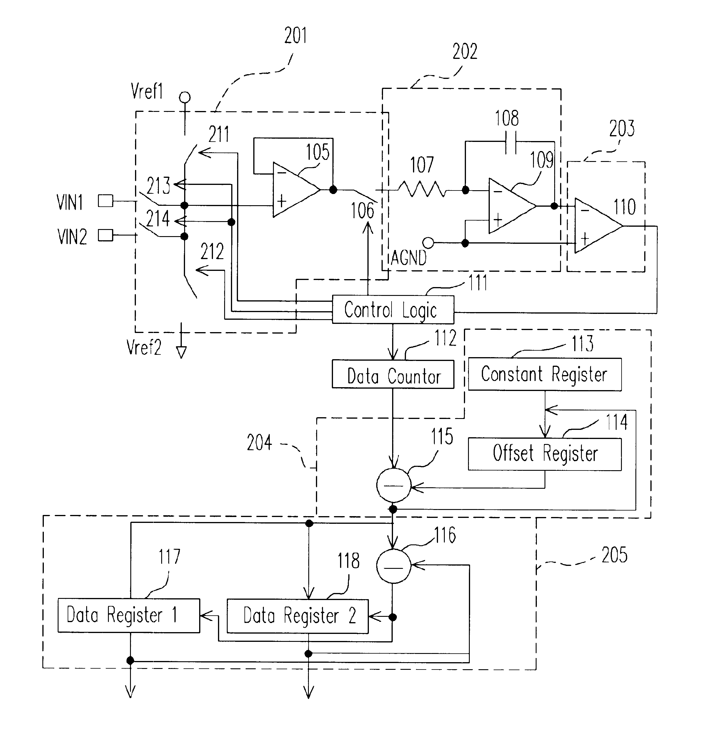
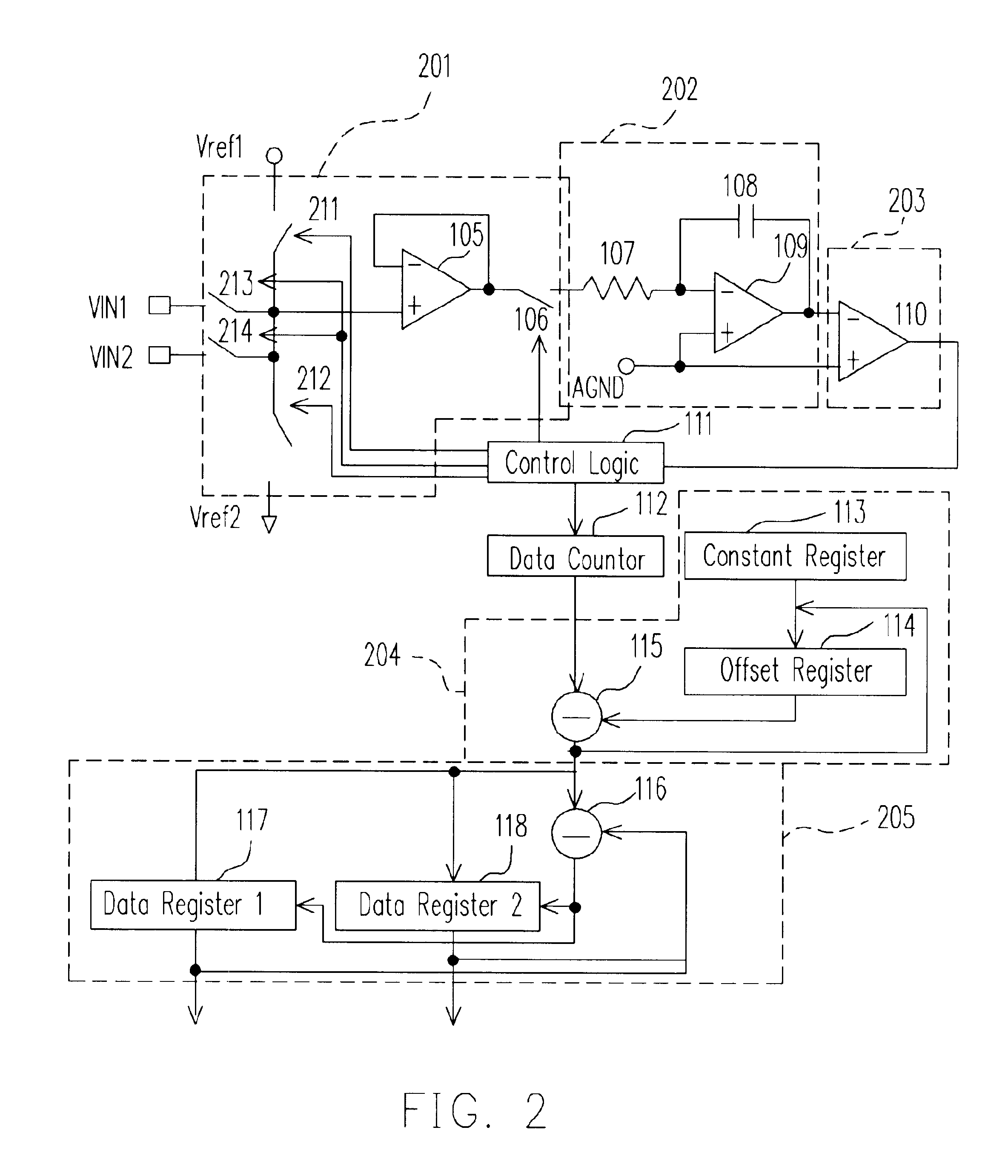
[0041]Referring to FIG. 2, it is a circuit diagram illustrating a dual slope analog-to-digital converter (ADC) according to one preferred embodiment of the present invention. A multi-channel dual slope analog-to-digital converter (ADC) is provided in this present invention. The circuit of this present invention includes an input circuit 201, an integrator 202, a comparator 203, a control logic 111, and a data counter 112. The circuit of this present invention further includes an offset cancellation logic 204 and a hysteresis logic 205. The control logic 111 determines input voltage for the input amplifier 105, after the processed signal is integrated, the comparator 203 comes into play. The offset cancellation logic 204 couples to the data counter 112, which is controlled by the control logic 111. Whereas the hysteresis logic 205 is coupled to the offset cancellation logic 204. On the other hand, the control logic 111 selects one of the input voltage levels, in order to process vari...


PUM


Abstract

A multi-channel dual slope analog-digital converter with offset cancellation an hysteresis input is provided in the present invention, wherein a charge reset period and an auto zero period are eliminated, so as to shorten cycle time. An offset cancel capacitor is also eliminated, so that large chip area is avoided. With inserting a dummy cycle in between each measurement cycle, coupling error can be avoided between different conversion channels. Also, hysteresis property of a Schmitt comparator in the comparator unit manages to filter out minute residual voltage offset, so that the output of converter retains its residual voltage level. A multi-channel dual slope analog-digital converting method is also provided in the invention.

Description

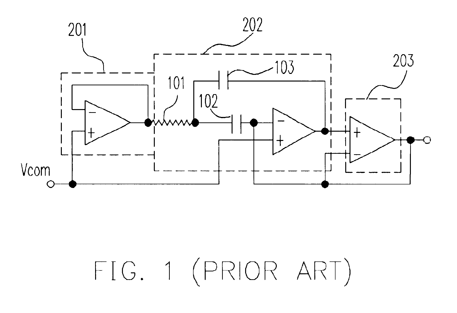
BACKGROUND OF INVENTION[0001]1. Field of the Invention[0002]This invention generally relates to a multi-channel dual slope analog-to-digital converting circuit and method thereof, and more particularly to a multi-channel dual slope analog-to-digital converting circuit and method thereof having offset cancellation logic and hysteresis logic.[0003]2. Description of Related Art[0004]A dual slope analog-to-digital converter (ADC) having zero-reset phase is provided in a conventional scheme.[0005]The dual slope ADC uses a correction voltage to eliminate residual offset voltage that is generated during integrating phase and discharge phase. In the conventional scheme, a comparator that is negative feedback connected manages to rapidly reset the output of an integrator, and the correction voltage is stored in the integrating capacitor and another capacitor coupling to the integrating operational amplifier. Where the devices and operation of which scheme is described as follows:FIG. 1 illus...

Claims


Application Information

Patent Timeline
Patent Type & Authority Patents(United States)
IPC IPC(8): H03M1/06H03M1/10H03M1/12H03M1/52
CPCH03M1/0697H03M1/52H03M1/1225
Inventor KOIKE, HIDCHARU
Owner WINBOND ELECTRONICS CORP
Learn More