
Dislocation reduction in non-polar gallium nitride thin films

a gallium nitride and thin film technology, applied in the field of semiconductor materials, can solve problems such as fixed sheet charge formation, and achieve the effect of reducing threading dislocations and gan films

Inactive Publication Date: 2005-05-31
RGT UNIV OF CALIFORNIA
View PDF20 Cites 139 Cited by
  • Summary
  • Abstract
  • Description
  • Claims
  • Application Information

AI Technical Summary

Benefits of technology

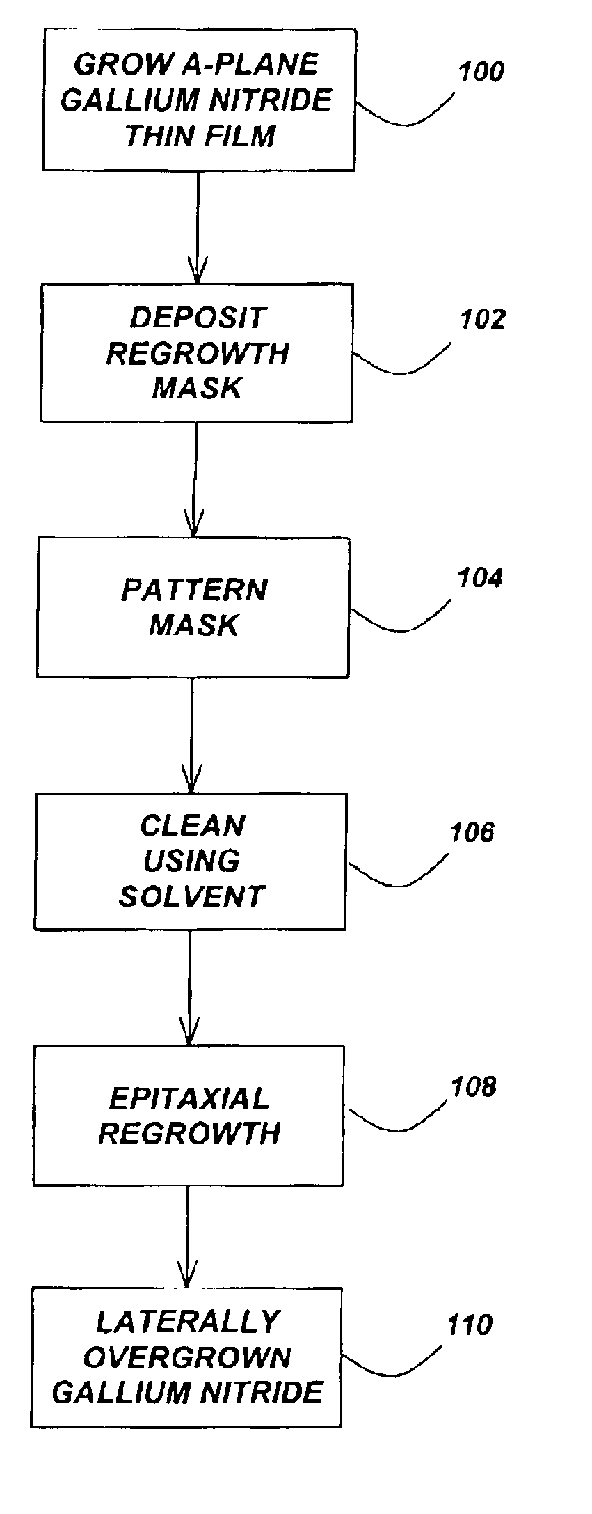
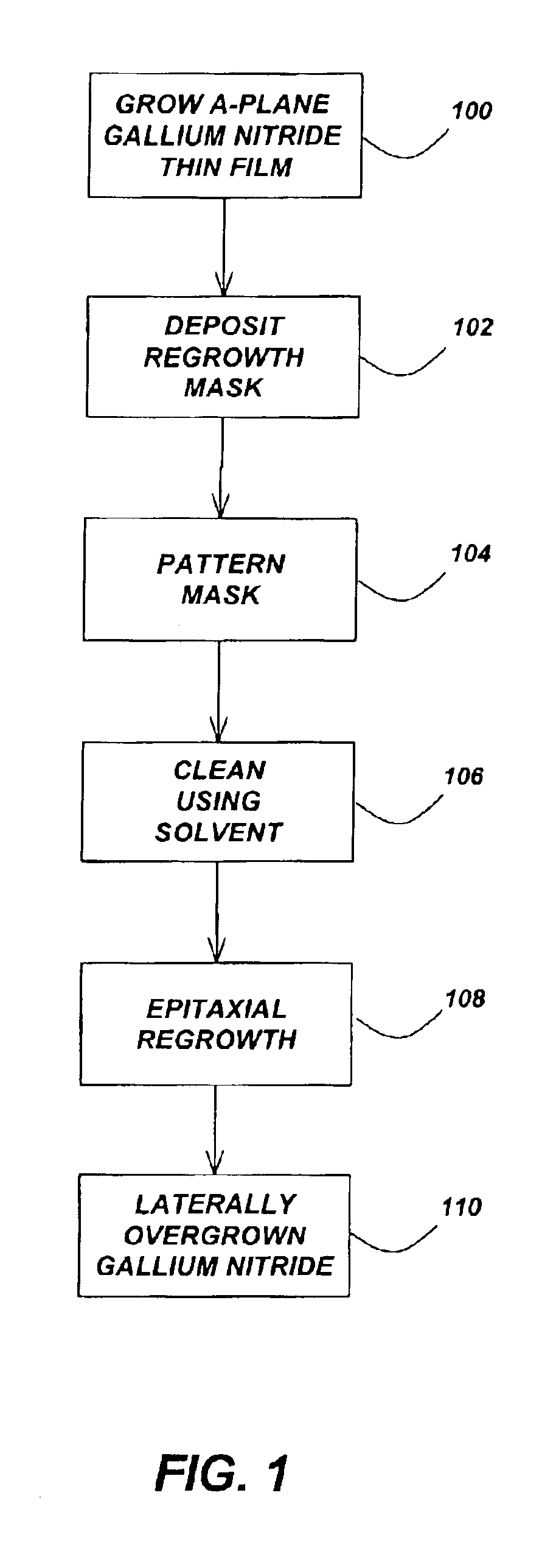
[0014]Lateral epitaxial overgrowth of non-polar (11{overscore (2)}0) a-plane GaN thin films reduces threading dislocations in the GaN films. First, a thin patterned dielectric mask is applied to the seed layer. Second, a selective epitaxial regrowth is performed to achieve a lateral overgrowth based on the patterned mask. Upon regrowth, the GaN films initially grow vertically through openings in the dielectric mask before laterally overgrowing the mask in directions perpendicular to the vertical growth direction. Threading dislocations are reduced in the overgrown regions by (1) the mask blocking the propagation of dislocations vertically into the growing film and (2) the bending of dislocations through the transition from vertical to lateral growth.

Problems solved by technology

These polarization-induced electric fields affect the performance of current state-of-the-art optoelectronic and electronic nitride devices.
Discontinuities in total polarization result in the formation of fixed sheet charges at the corresponding interfaces or surfaces.

Method used


Image

  • Dislocation reduction in non-polar gallium nitride thin films
  • Dislocation reduction in non-polar gallium nitride thin films
  • Dislocation reduction in non-polar gallium nitride thin films

Examples


Embodiment Construction

[0021]In the following description of the preferred embodiment, reference is made to the accompanying drawings which form a part hereof, and in which is shown by way of illustration a specific embodiment in which the invention may be practiced. It is to be understood that other embodiments may be utilized and structural changes may be made without departing from the scope of the present invention.

[0022]Overview

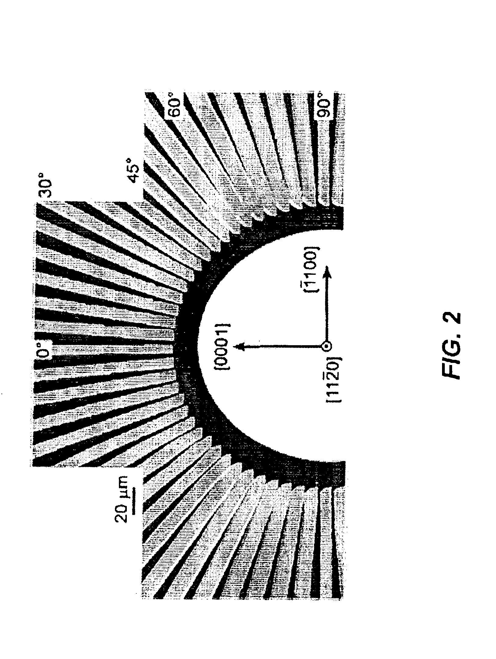
[0023]The present invention reduces threading dislocation densities in a-GaN through the lateral overgrowth of a planar heteroepitaxial “seed” layer. Lateral overgrowth techniques require a processing step between two MOCVD growths, an initial heteroepitaxial growth and a regrowth that constitutes the lateral overgrowth. First, a thin patterned dielectric mask is applied to the seed layer. Upon regrowth, the GaN initially grows vertically through openings in the dielectric mask before laterally overgrowing the mask in directions perpendicular to the vertical growth direction. ...


PUM

PropertyMeasurementUnit
dislocation densitiesaaaaaaaaaa
threading dislocation densitiesaaaaaaaaaa
NON-POLARaaaaaaaaaa

Abstract

Lateral epitaxial overgrowth of non-polar (11{overscore (2)}0) a-plane GaN seed layers reduces threading dislocations in the GaN films. First, a thin patterned dielectric mask is applied to the seed layer. Second, a selective epitaxial regrowth is performed to achieve a lateral overgrowth based on the patterned mask. Upon regrowth, the GaN films initially grow vertically through openings in the dielectric mask before laterally overgrowing the mask in directions perpendicular to the vertical growth direction. Threading dislocations are reduced in the overgrown regions by (1) the mask blocking the propagation of dislocations vertically into the growing film and (2) the bending of dislocations through the transition from vertical to lateral growth.

Description

CROSS-REFERENCE TO RELATED APPLICATIONS[0001]This application claims the benefit under 35 U.S.C. §119(e) of the following co-pending and commonly-assigned U.S. Provisional Patent Application Ser. No. 60 / 372,909, entitled “NON-POLAR GALLIUM NITRIDE BASED THIN FILMS AND HETEROSTRUCTURE MATERIALS,” filed on Apr. 15, 2002, by Michael D. Craven, Stacia Keller, Steven P. DenBaars, Tal Margalith, James S. Speck, Shuji Nakamura, and Umesh K. Mishra, which application is incorporated by reference herein.[0002]This application is related to the following co-pending and commonly-assigned U.S. utility patent applications:[0003]Ser. No. 10 / 413,690, entitled “NON-POLAR (Al,B,In,Ga)N QUANTUM WELL AND HETEROSTRUCTURE MATERIALS AND DEVICES,” filed on Apr. 15, 2003, by Michael D. Craven, Stacia Keller, Steven P. DenBaars, Tal Margalith, James S. Speck, Shuji Nakamura, and Umesh K. Mishra, which application claims the benefit under 35 U.S.C. §119(e) of co-pending and commonly-assigned U.S. Provisional...

Claims


Application Information

Patent Timeline
Patent Type & Authority Patents(United States)
IPC IPC(8): C30B25/18C30B25/10C30B29/60C30B25/02C30B25/04C30B29/00H01L21/02H01L21/205C23C16/04C30B29/38C30B29/40H01S5/343
CPCC30B25/02H01L21/02647C30B25/105C30B25/18C30B29/403C30B29/406C30B29/605H01L21/0237H01L21/0242H01L21/02433H01L21/02458H01L21/0254H01L21/02609H01L21/0262H01L21/02639C30B25/04
Inventor CRAVEN, MICHAEL D.DENBAARS, STEVEN P.SPECK, JAMES STEPHEN
Owner RGT UNIV OF CALIFORNIA
Learn More