Group III nitride compound semiconductor device
a semiconductor and compound technology, applied in the direction of semiconductor devices, basic electric elements, electrical appliances, etc., can solve the problems that metal nitride with such a large thickness has never been provided as a raw material for semiconductor-producing industrial products, and achieves good crystallinity, good crystallinity, and low lattice mismatching
- Summary
- Abstract
- Description
- Claims
- Application Information
AI Technical Summary
Benefits of technology
Problems solved by technology
Method used
Image
Examples
first embodiment
(First Embodiment)
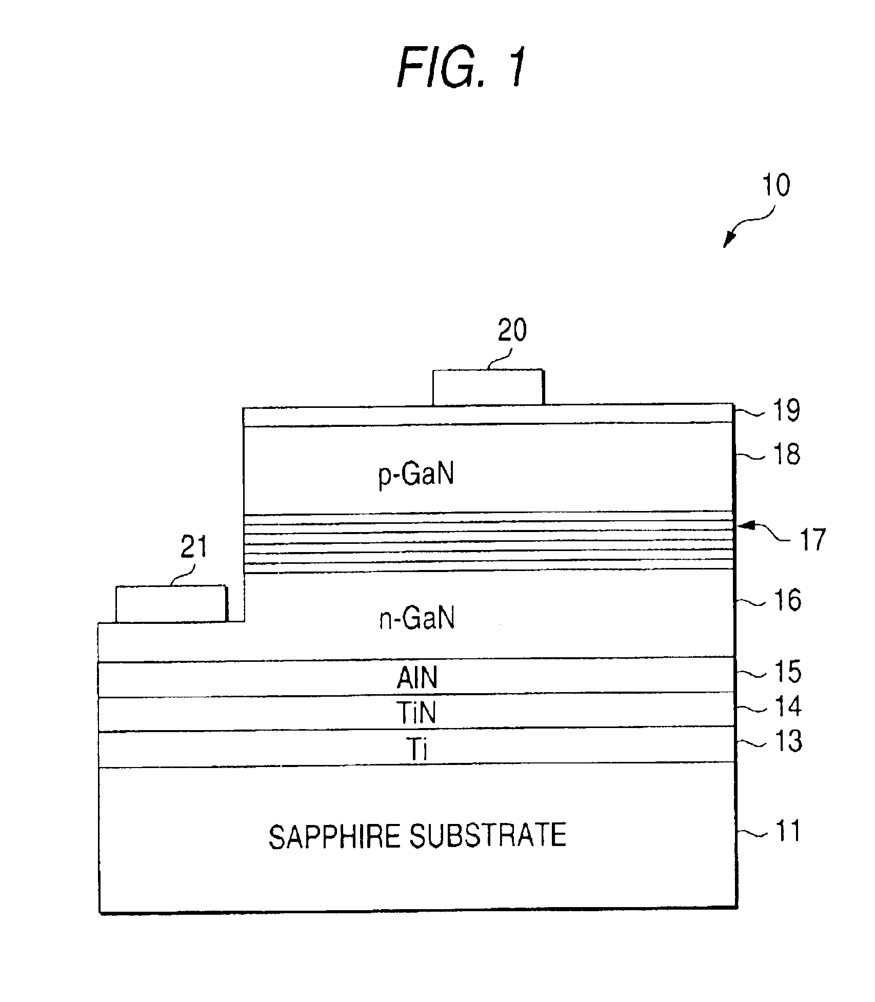
[0035]This embodiment is a light-emitting diode 10, the configuration of which is shown in FIG. 1.
[0036]Specifications of respective layers are as follows.
[0037]
Layer Component Dopantp-type layer 18 p-GaN MgLayer 17 including aincluding InGaN layerlight-emitting layern-type layer 16n-GaNSiBuffer layer 15AlNTiN layer 14TiNTi layer 13TiSubstrate 11sapphire
[0038]The n-type layer 16 may be of a double-layered structure with an n− layer of a low electron density on the side of the layer 17 including the light-emitting layer and an n+ layer of a high electron density on the buffer layer 15 side. The later is called n-type contact layer.
[0039]The layer 17 including the light-emitting layer are not limited to the superlattice structure. A single or double hetero type structure, a homo-junction type structure, or the like, may be used as the configuration of the light-emitting device. A single quantum well structure may be also used.
[0040]A layer of AlXInYGa1-X-YN (includin...
second embodiment
(Second Embodiment)
[0048]FIG. 2 shows a light-emitting diode 22 according to a second embodiment. Incidentally, parts the same as those in the first embodiment are referenced correspondingly and the description of the parts will be therefore omitted.
[0049]
Layer Component Dopantp-type layer 18 p-GaN MgLayer 17 including aincluding InGaN layerlight-emitting layern-type layer 16n-GaNSiBuffer layer 15AlNTiN layer 14TiNTi layer 13TiSubstrate 25silicon single crystal(111)
[0050]The method of growing the TiN layer 14 and layers after the TiN layer 14 on the (111) surface of Si is the same as that in the first embodiment.
[0051]Incidentally, the Si substrate layer 25 can be used as an n-type electrode because it has electrically conductive characteristic. Incidentally, the AlN buffer layer 15 may be formed by an MOCVD method or by any other method. Further, an Al layer with a film thickness of 10 nm (100 Å) may be formed between the Si substrate and Ti.
third embodiment
(Third Embodiment)
[0052]FIG. 3 shows a semiconductor device according to a third embodiment of the present invention. The semiconductor device in this embodiment is a light-emitting diode 32. Incidentally, parts the same as those in FIG. 2 are referenced correspondingly and the description of the parts will be therefore omitted.
[0053]Specifications of respective layers are as follows.
[0054]
Layer Component Dopantn-type layer 28 n-GaN SiLayer 17 including aincluding InGaN layerlight-emitting layerp-type layer 26p-GaNMgBuffer layer 15AlNTiN layer 14TiNTi layer 13TiSubstrate 25silicon single crystal(111)
[0055]As shown in FIG. 3, the p-type layer 26, the layer 17 including the light-emitting layer and the n-type layer 28 are grown successively on the buffer layer 15. Thus, a light-emitting diode 32 is formed. In the case of this device 32, the light-transmissible electrode (see the reference numeral in FIG. 2) can be omitted because the n-type layer 28 low in resistance value is provided...
PUM
| Property | Measurement | Unit |
|---|---|---|
| thickness | aaaaa | aaaaa |
| thickness | aaaaa | aaaaa |
| thickness | aaaaa | aaaaa |
Abstract
Description
Claims
Application Information
 - R&D
- Intellectual Property
- Life Sciences
- Materials
- Tech Scout
- Unparalleled Data Quality
- Higher Quality Content
- 60% Fewer Hallucinations
Browse by: Latest US Patents, China's latest patents, Technical Efficacy Thesaurus, Application Domain, Technology Topic, Popular Technical Reports.
© 2025 PatSnap. All rights reserved.Legal|Privacy policy|Modern Slavery Act Transparency Statement|Sitemap|About US| Contact US: help@patsnap.com


