
Method and related circuitry for buffering output signals of a chip with even number driving circuits

Active Publication Date: 2005-05-03
VIA TECH INC
View PDF4 Cites 3 Cited by
  • Summary
  • Abstract
  • Description
  • Claims
  • Application Information

AI Technical Summary

Benefits of technology

[0011]It is therefore a primary objective of the claimed invention to provide a method and related circuit that can compensate waveform (or duty cycle) distortion caused by semiconductor process imperfection when making inverters.
[0012]The principle revealed by the claimed invention is to use an even number of inverter driving circuits to produce driving signals, the equivalent load of every inverter remaining the same. In this way, the driving capability difference caused by inverter mismatch can be compensated and corrected through circuit design.

Problems solved by technology

There are usually numerous logic gates in chips to perform certain functions; however, in practical circuit operation, logic gates also introduce some imperfect factors such that a signal profile of the logic circuit is not as expected.
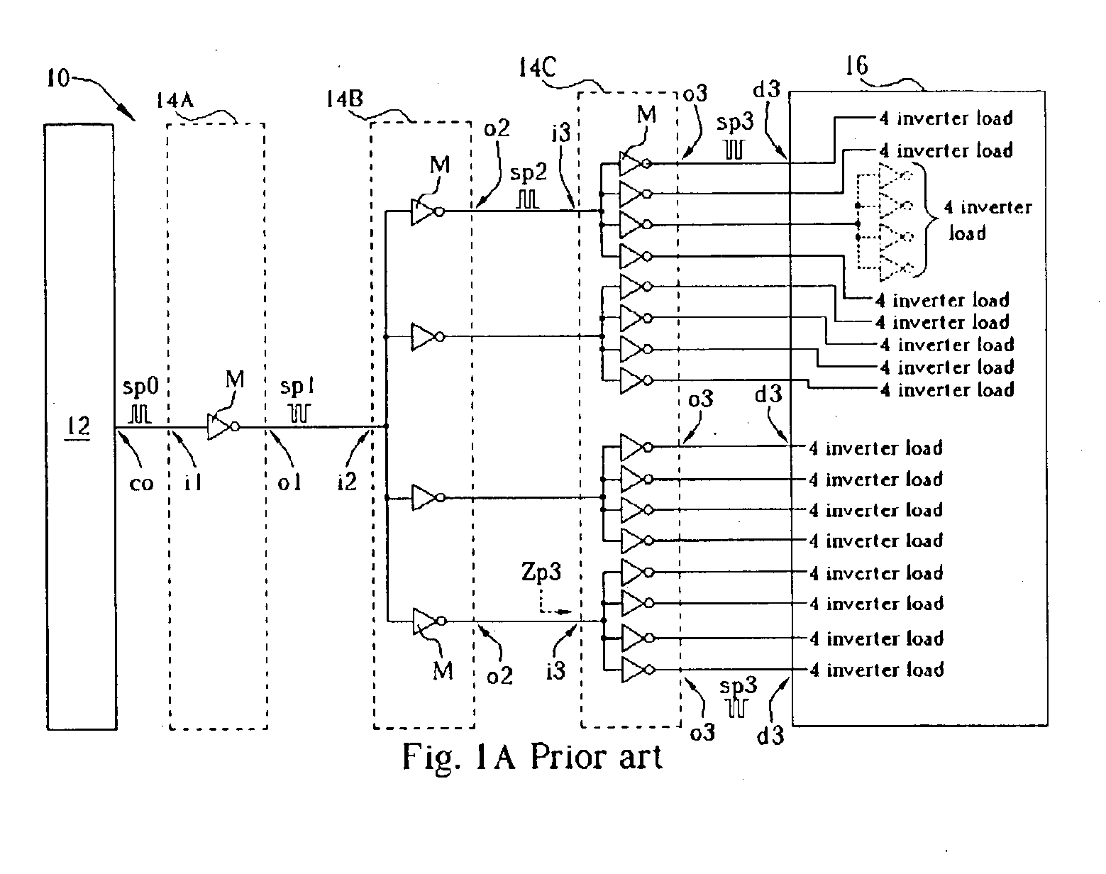
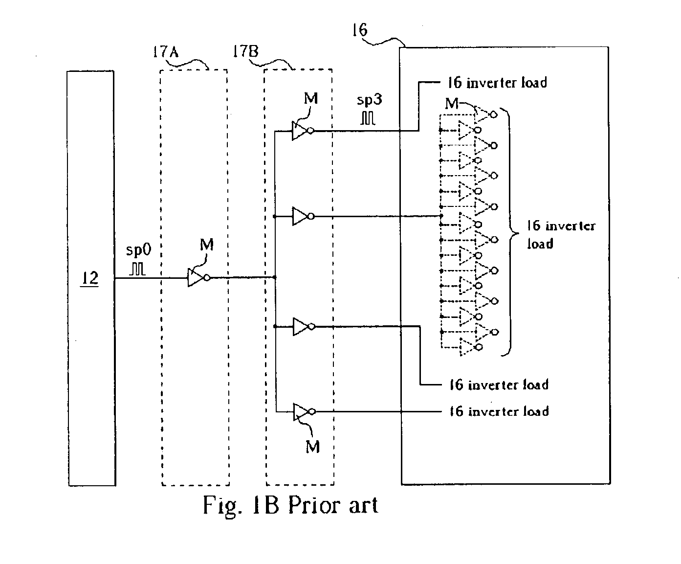
However, the allocation of a plurality of inverters M in chip 10, results in signal distortion that causes duty cycle distortion of signal sp3 because of inverter M mismatch.
However, if the transistors Qn, Qp of the inverter M are not matched for charge and discharge, the waveform quality of the output waveform at the node Nop will be affected.
A mismatched semiconductor process makes the capability of driving discharge current of the transistor Qn less than the capability of driving charge current of the transistor Qp.
In other words, when the inverter M has mismatched transistors, the waveform of driving output for inverter M will be distorted, and cannot have the same duty cycle as the input waveform.
This type of duty cycle distortion will lead to a timing error, waveform distortion in logic circuits, and even errors in circuit function.
Because of the limited precision of semiconductor processes, inverter mismatch is not impossible.
Mismatch will cause waveform distortion and limit the margin of error allowed during circuit operation.

Method used


Image

  • Method and related circuitry for buffering output signals of a chip with even number driving circuits
  • Method and related circuitry for buffering output signals of a chip with even number driving circuits
  • Method and related circuitry for buffering output signals of a chip with even number driving circuits

Examples


Embodiment Construction

[0021]In order to compensate inverter mismatch caused by semiconductor process errors, the present invention reveals two driving circuit design principles to avoid waveform duty cycle distortion caused by inverter mismatch. First, the present invention uses an even number of inverter driving circuits to produce final driving signals level by level. And second, the present invention maintains consistency of equivalent output load for inverters in every driving circuit. To illustrate the above principles in detail, we use the following embodiment as an example.

[0022]Please refer to FIG. 4. FIG. 4 is a circuit diagram of a chip 20 according to the present invention. An output signal of an output end op0 of a circuit 22 becomes an input signal s0 of a driving circuit 24A. There is one input end ip1 and an output end op1 in the driving circuit 24A, and also one inverter T as a driving unit to match the single output end op1. An input end of this inverter is connected to the input end ip1...


PUM


Abstract

A method and related circuitry for driving output signals of a chip is disclosed. The method includes driving output signals with an even number of inverter driving circuits, and keeping an equivalent load of each inverter of the driving circuits substantially identical by keeping impedances of each driving circuit substantially identical.

Description

BACKGROUND OF THE INVENTION[0001]1. Field of the Invention[0002]The present invention provides a method and related circuit for driving a chip to output signals, and more particularly, a method and related circuit that use a plurality of inverters with equivalent loads to form an even number inverter driving circuit to drive output signals.[0003]2. Description of the Prior Art[0004]In modern society, microprocessor chips that process information are one of the most important hardware components for various information products. There are usually numerous logic gates in chips to perform certain functions; however, in practical circuit operation, logic gates also introduce some imperfect factors such that a signal profile of the logic circuit is not as expected. So it is one of the major topics for the modern IT industry to construct circuit design that minimizes the effect of these imperfections.[0005]Please refer to FIG. 1A. FIG. 1A is a circuit diagram for a prior art chip 10. In t...

Claims


Application Information

Patent Timeline
IPC IPC(8): H03K19/0175H03K19/003H03K19/00H04L25/02
CPCH03K19/0005H03K19/00323H04L25/0286H03K19/017545H04L25/0278H03K19/00369
Inventor WEI, YI-KUANGHUANG, CHIA-CHUNKUO, CHI-REN
Owner VIA TECH INC
Learn More