Scanning switch transistor for solid-state imaging device

a solid-state imaging and switching transistor technology, applied in the field of solid-state imaging devices, can solve the problems of difficult generation of vertical stripe-shaped fixed pattern noise (fpn), and achieve the effect of improving detection sensitivity and reducing the parasitic capacity of horizontal signal lines

Inactive Publication Date: 2005-03-29
SONY CORP
View PDF9 Cites 10 Cited by
  • Summary
  • Abstract
  • Description
  • Claims
  • Application Information

AI Technical Summary

Benefits of technology

In view of the aforesaid aspect, it is an object of the present invention to provide a solid-state imaging device wherein a detection sensitivity can be improved by decreasing a parasitic capacity of a horizontal signal line.

Problems solved by technology

Further, since the load is the capacity element 7, signal charges cannot be fluctuated less unlike the load MOS transistor, and hence a vertical stripe-shaped fixed pattern noise (FPN) is difficult to be generated.

Method used


Image

  • Scanning switch transistor for solid-state imaging device
  • Scanning switch transistor for solid-state imaging device
  • Scanning switch transistor for solid-state imaging device

Examples


first embodiment

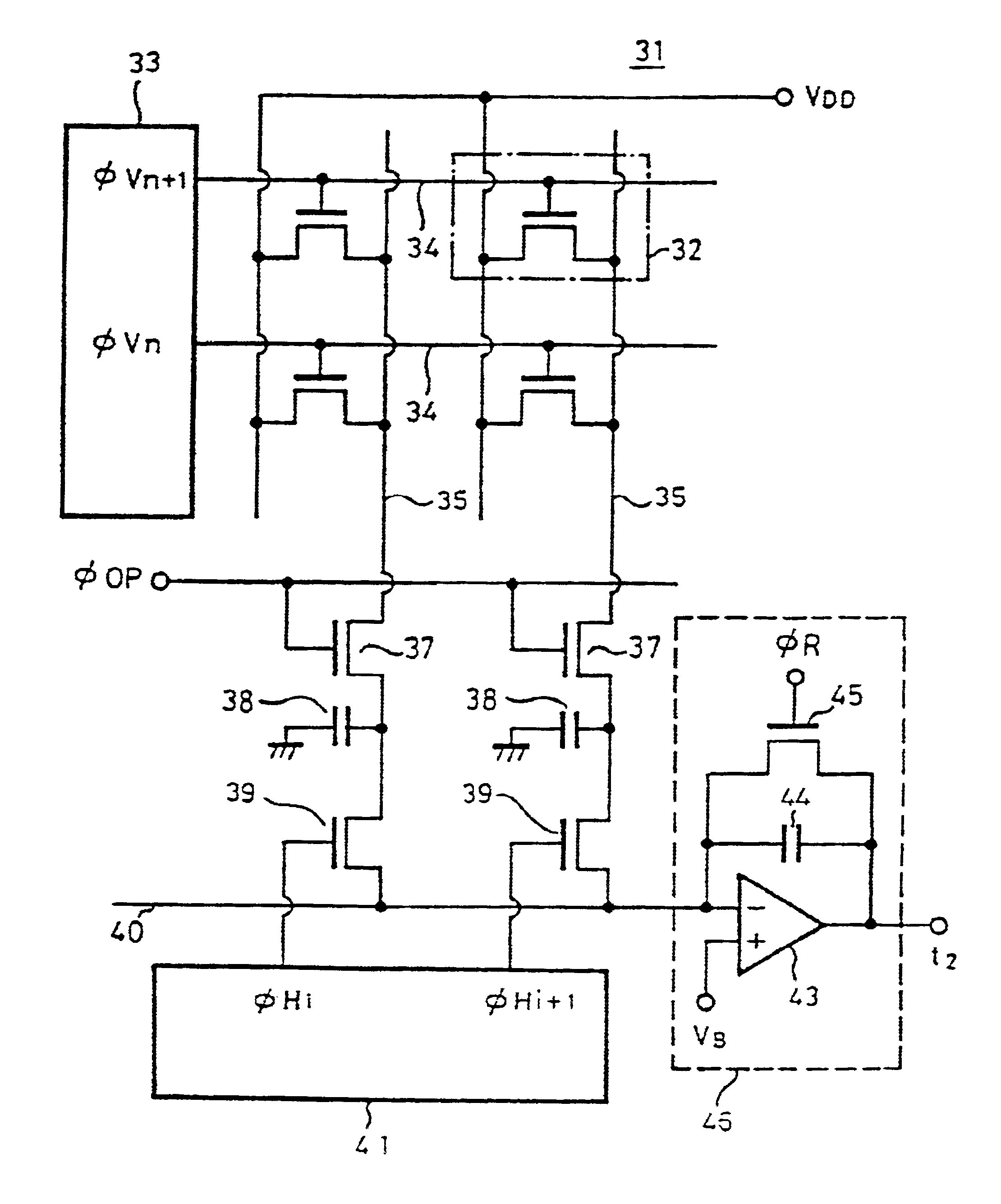
FIGS. 3 and 4 show a solid-state imaging device according to the present invention which is applied to a load capacity operation system amplifying type solid-state imaging device.

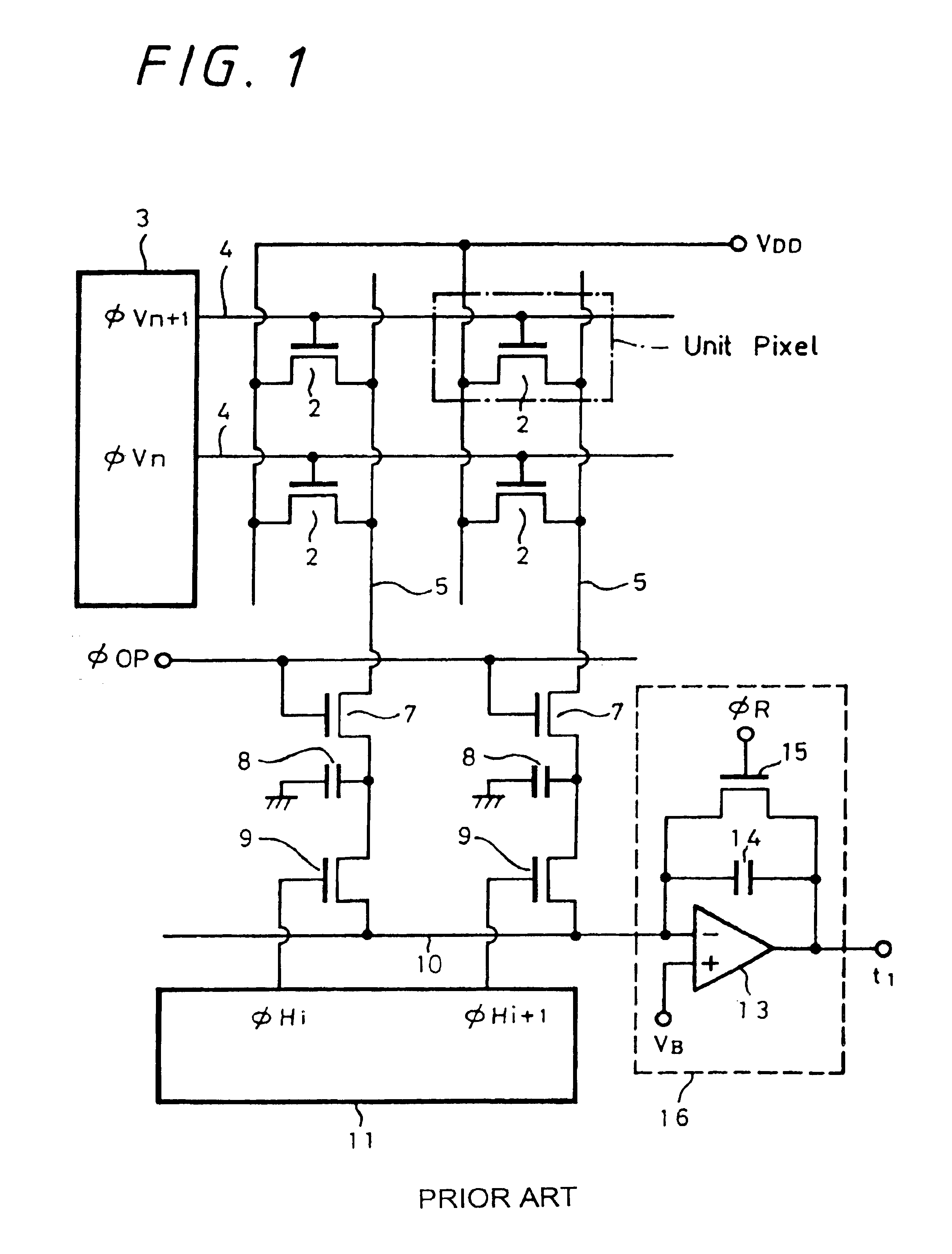
The solid-state imaging device shown in FIG. 3 has an equivalent circuit arrangement similar to that shown in FIG. 1. In FIG. 3, reference numeral 31 generally denotes an amplifying type solid-state imaging device. Reference numeral 32 denotes a light-receiving element comprising a unit pixel (cell), e.g., pixel transistor, i.e., pixel MOS transistor in this embodiment. A plurality of pixel MOS transistors 32 are arranged in a matrix fashion. Reference numeral 34 denotes vertical scanning lines connected to gates of the pixel MOS transistors 32 provided at every row. The vertical scanning lines 34 are connected to a vertical scanning circuit 33, and supplied with vertical scanning signals, i.e., vertical scanning pulses θV [θV1, . . . θVn, θVn+1, . . . ] sequentially from the vertical scanning circuit 33. T...


PUM


Abstract

A solid-state imaging device can improve a detection sensitivity of a signal detecting means by decreasing a parasitic capacity of a horizontal signal line. In a solid-state imaging device in which a plurality of pixels are arranged in a matrix fashion, a pixel signal is flowed through a horizontal switch (39) to a horizontal signal line (40) as a signal charge, and a signal is outputted by a signal detecting means connected to the end off the horizontal signal line (40), an insulating gate-type field-effect transistor comprising the horizontal switch (39) includes channels extended at least in two directions between its source electrode connected to the horizontal signal line (40) and other drain electrode.

Description

BACKGROUND OF THE INVENTIONThe present invention relates to a solid-state imaging device, and more particularly to an amplifying type solid-state imaging device or a solid-state imaging device such as a MOS (metal oxide semiconductor) solid-state imaging device.As a demand that a solid-state imaging device becomes high in resolution is increased, an internal amplifying type solid-state imaging device has hitherto been developed, and other MOS type solid-state imaging devices also have been known so far.As the internal amplifying type solid-state imaging device, there are mainly known a static induction transistor (SIT), an amplifying type MOS imager (AMI), a charge-modulation device (CMD), and various imaging device structures such as a BASIS (base-stored image sensor) using bipolar transistors as pixels.The following amplifying type solid-state imaging device is known as one of such internal amplifying type solid-state imaging devices. This amplifying type solid-state imaging devic...

Claims


Application Information

Patent Timeline
Patent Type & Authority Patents(United States)
IPC IPC(8): H01L27/146H04N3/15H04N5/374H04N5/376H04N5/378
CPCH04N3/1575H01L27/14643H04N25/76
Inventor YONEMOTO, KAZUYA
Owner SONY CORP
Why Eureka
Try Eureka