Film forming unit

Inactive Publication Date: 2005-03-29
TOKYO ELECTRON LTD
View PDF13 Cites 25 Cited by
  • Summary
  • Abstract
  • Description
  • Claims
  • Application Information

AI Technical Summary

Benefits of technology

The present invention has been made in view of the aforementioned points, and it is a first object thereof to perfectly remove contamination adhered on a discharging port of a coating solution discharge nozzle even if the disharging port has a minute hole diameter, in order to form a preferred and uniform film of a coating solution on the surface of substrate. It is a second object of the present invention to form a film of a coating solution having a constant thickness by controlling variation in the volume of processing fluid discharged from a coating solution discharge nozzle onto a substrate.
According to a fifth aspect of the present invention, a film forming unit of the present invention includes the coating solution discharge nozzle having a flow path for the coating solution; a discharging port connected to the flow path for the coating solution for discharging the coating solution in a line form having a very small diameter; and a filter provided to cross the flow path for the coating solution for removing air bubbles from the coating solution. In this case, variation in discharge pressure of the processing fluid which is caused by the presence of air bubbles included in the processing fluid, and the like are suppressed. This allows the stable supply of the processing fluid for the substrate, resulting in improving uniformity of a film thickness of a solution layer. In this point, it is desirable that the filter is made of a porous resin.

Problems solved by technology

If the discharge flow path has a water repellant finish against the coating solution, this causes hard adhering contamination on the discharge flow path, resulting in reduction in number of cleaning.

Method used


Image

  • Film forming unit
  • Film forming unit
  • Film forming unit

Examples


Embodiment Construction

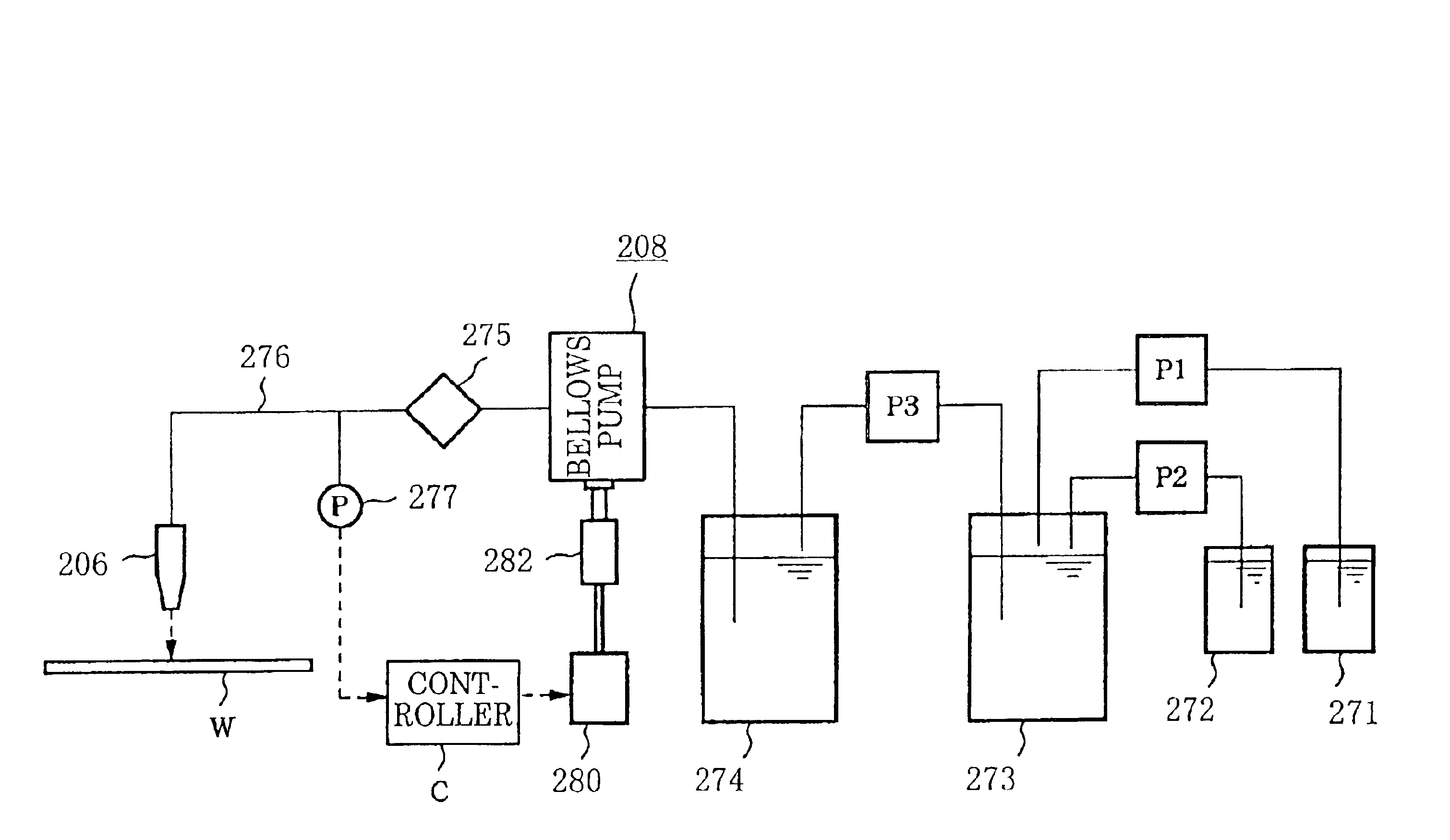
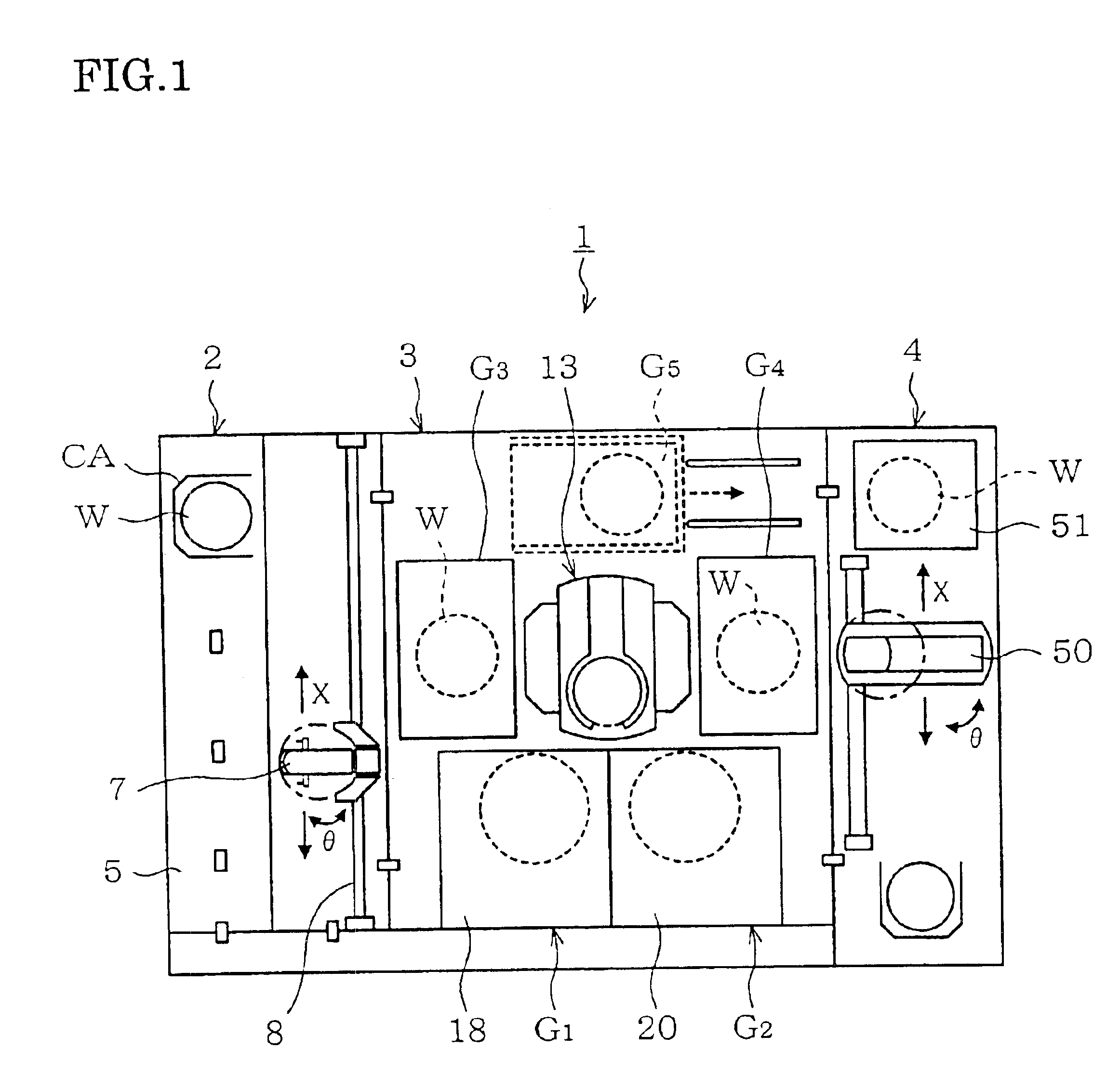
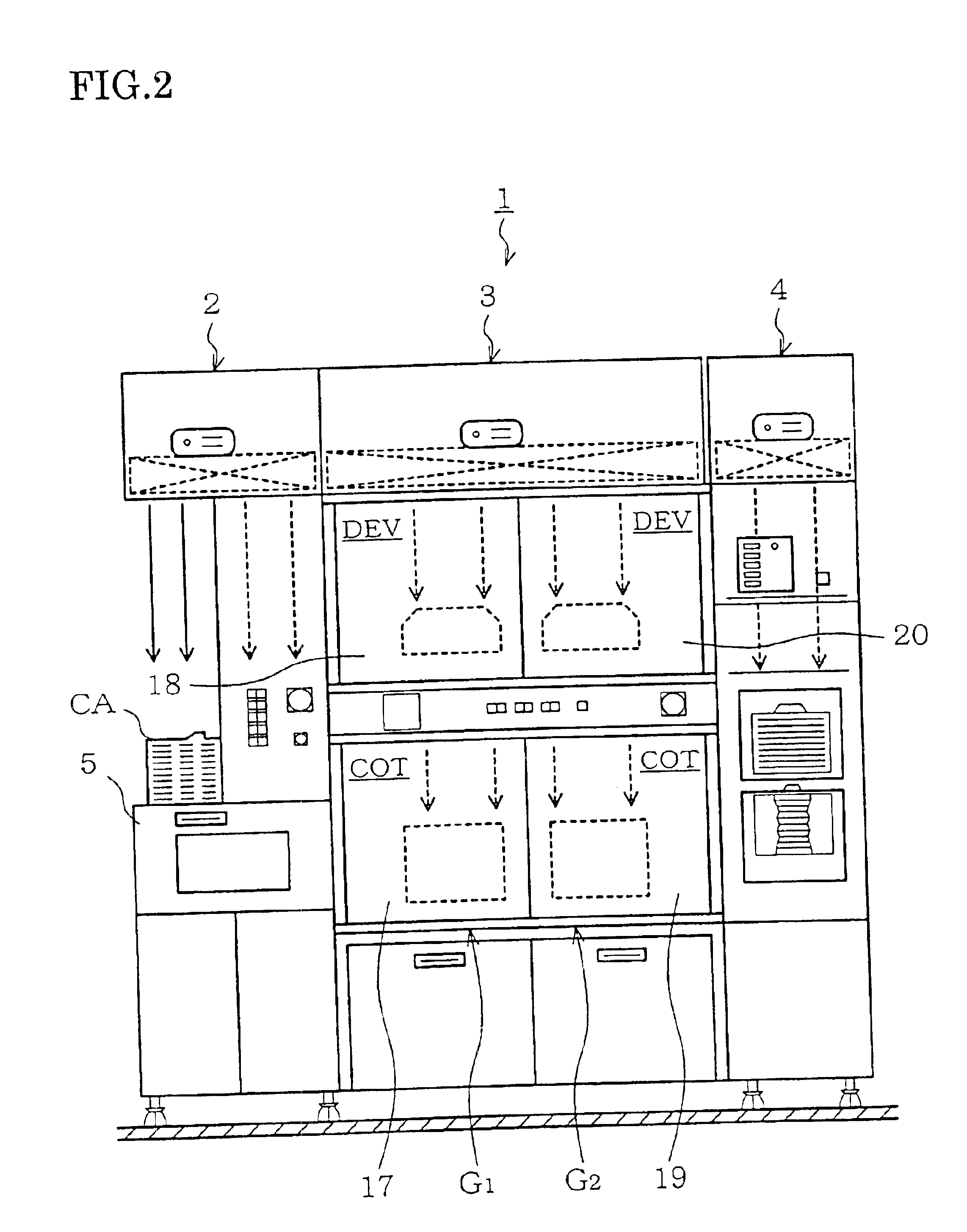
Preferred embodiments of the present invention will be below described. FIG. 1 is a plane view of a coating and developing system 1 having a resist coating unit according to the embodiment. FIG. 2 is a front view of the coating and developing system 1, and FIG. 3 is a back view of the coating and developing system 1.

As shown in FIG. 1, the coating and developing system 1 has a configuration of integral connection of a cassette station 2 for carrying wafers W, for example, 25 wafers W in cassette between an outside source and the coating and developing system 1 and carrying the wafer W into and from a cassette CA; a processing station 3 consisting of a multistage arrangement of various processing units respectively providing predetermined processings in sheet form in the coating and developing process; and an interface section 4 taking in / taking out the wafer from a not shown aligner arranged next to the processing station 3.

In the cassette station 2, a plurality of cassettes C are r...


PUM


Abstract

The present invention is a film forming unit for discharging a coating solution from a coating solution discharge nozzle toward a substrate to form a layer on a surface of the substrate, which has a supply flow path for supplying a cleaning fluid to a discharge flow path continuing to a discharging port of the coating solution discharge nozzle. When the cleaning fluid is positively supplied directly to the discharge flow path of the coating solution discharge nozzle, the supply pressure of the cleaning fluid as well as the capability of cleaning is added. Therefore, further effective cleaning is attained in compare with the conventional case where a coating solution discharge nozzle is simply dipped into a cleaning fluid. In consequence, even when the discharging port of the nozzle is minute, it is possible to perfectly remove the contamination. This allows the discharge pressure to remain constant so as to form a uniform coating layer on the substrate.

Description

BACKGROUND OF THE INVENTION1. Field of the InventionThis invention relates to a film forming unit for forming a coating layer on a surface of a substrate.2. Description of the Related ArtIn the process for manufacturing semiconductor devices, for example, the photolithography process including resist coating processing for coating a resist solution on a wafer surface to form a resist layer, exposure processing for exposing to define a pattern on a wafer, developing treatment for developing the wafer having been exposed, and so on is performed with the respective processing devices to form a predetermined circuit pattern on the wafer.In the above resist coating processing, the resist solution is discharged from a coating solution discharge nozzle toward above of the wafer. The coating solution discharge nozzle is contaminated by the resist solution and the like and thus needed to clean as necessary.Conventionally, the coating solution discharge nozzle is cleaned with a cleaning fluid...

Claims


Application Information

Patent Timeline
IPC IPC(8): G03F7/16H01L21/00B05C11/08H01L21/027
CPCG03F7/16H01L21/6715H01L21/67051G03F7/162B05C11/08B05B15/55H01L21/027
Inventor KITANO, TAKAHIROMORIKAWA, MASATERUESAKI, YUKIHIKOISHIZAKA, NOBUKAZUKOGA, NORIHISATAKESHITA, KAZUHIROOOKUMA, HIROFUMIAKIMOTO, MASAMI
Owner TOKYO ELECTRON LTD
Why Eureka
Try Eureka