Common-mode and differential-mode compensation for operational amplifier circuits

a technology of differential mode and amplifier circuit, which is applied in the direction of differential amplifier, amplifier with semiconductor device/discharge tube, amplifier details, etc., can solve the problems of limiting the overall amplifier performance, lowering signal bandwidth and slew rate, and still different impedances,

Active Publication Date: 2005-03-15
INTERSIL INC
View PDF3 Cites 22 Cited by
  • Summary
  • Abstract
  • Description
  • Claims
  • Application Information

AI Technical Summary

Benefits of technology

In accordance with the present invention, a compensation scheme is provided for two interconnected amplifier circuits which allows independent frequency compensation of the common-mode and / or differential signal paths. This method can be used to stabilize differential circuits without compromising performance through over-compensation, and without any need to isolate the amplifiers from one another.

Problems solved by technology

If, for example, the common-mode signal path requires a higher value of CCOMP, then the differential signal path will be “over-compensated”, thus lowering signal bandwidths and slew rates and limiting overall amplifier performance.
However, the load impedance is still different for the two signal paths and some over-compensation is unavoidable.
Additionally, the connection to ground in the circuit of FIG. 3 has several undesirable properties.
These effects will compromise differential signal performance.

Method used


Image

  • Common-mode and differential-mode compensation for operational amplifier circuits
  • Common-mode and differential-mode compensation for operational amplifier circuits
  • Common-mode and differential-mode compensation for operational amplifier circuits

Examples


Embodiment Construction

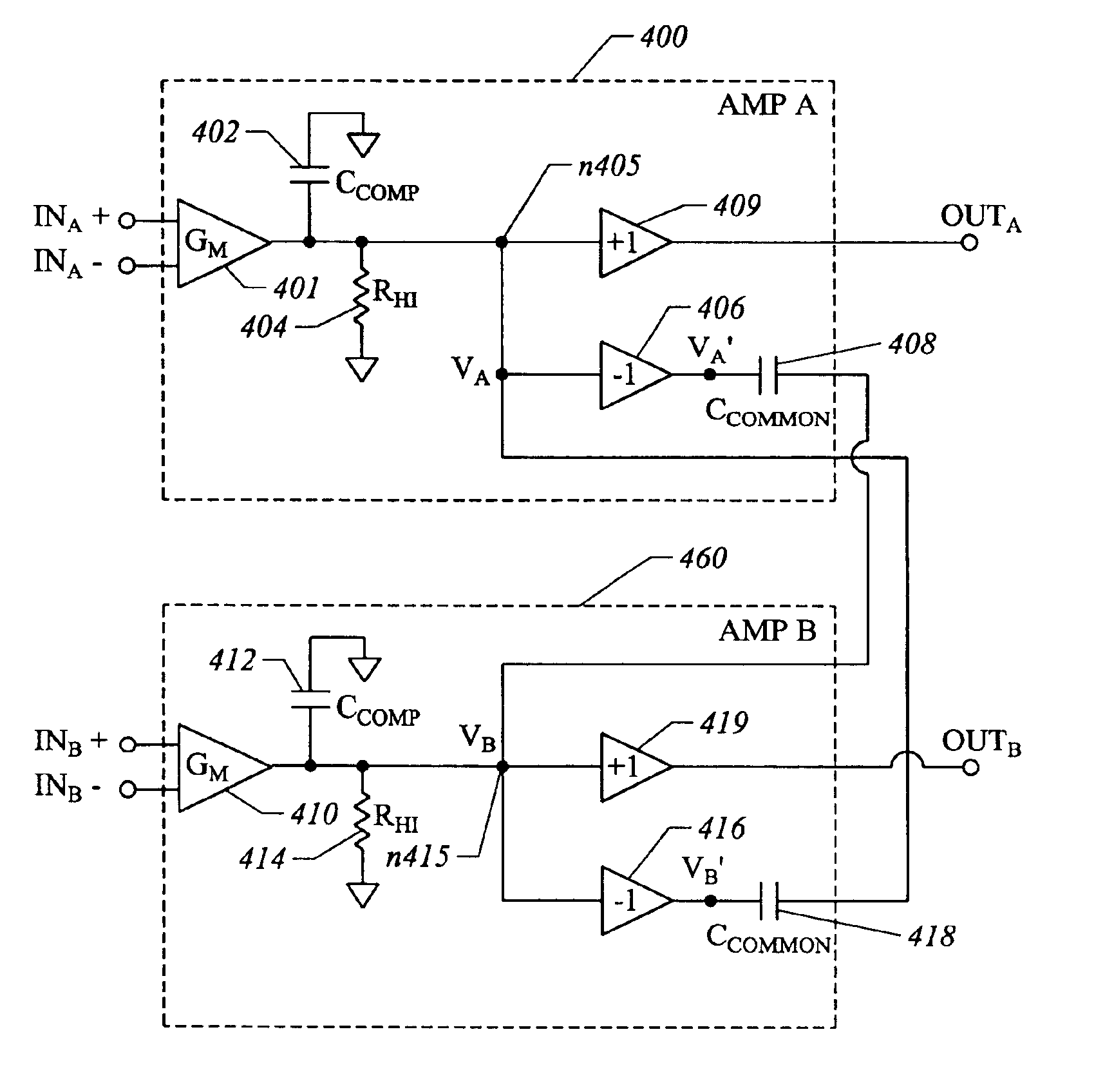
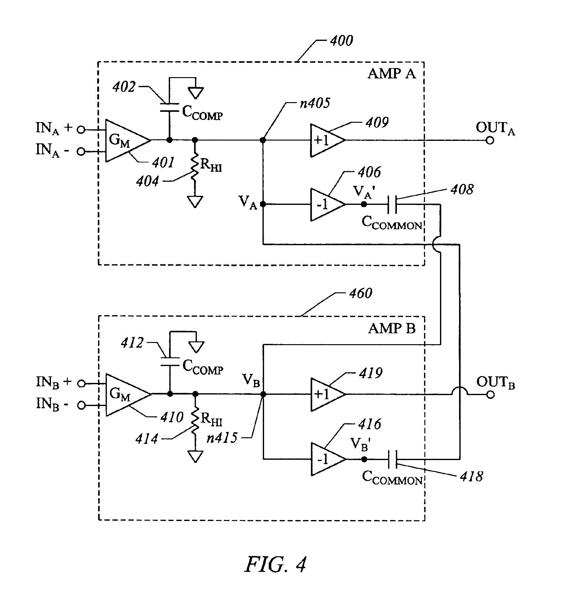
FIG. 4 shows an operational amplifier using a compensation technique in accordance with embodiments of the present invention. The circuit of FIG. 4 includes two amplifiers, AMPA 400 and AMPB 460. The amplifier AMPA 400 includes a transconductance amplifier 401, high impedance node resistor 404, compensation capacitor 402, and output buffer 409, similar to the components of FIG. 1. Similarly, amplifier AMPB 460 includes a transconductance amplifier 410, high impedance node resistor 414, compensation capacitor 412, and output buffer 419, as in FIG. 1.

Unlike the components of FIG. 1, the amplifier AMPA 400 further includes an inverter 406 and common mode compensation capacitor CCOMMON 408 connected in series. The input of the inverter 406 is connected to the gain node n405 of the amplifier AMPA 400, and the output of the capacitor CCOMMON 408 is connected to the gain node n415 of the amplifier AMPB 460. Similarly, the amplifier AMPB 460 includes an inverter 416 and common mode compensa...


PUM


Abstract

An amplifier is configured to provide both common-mode and differential-mode compensation to ensure stability in telecommunications circuits or other circuits where both common mode and differential mode signal paths are provided. The amplifier includes two interconnected operational amplifiers AMPA and AMPB. Common mode compensation is provided by connecting one or more capacitors with a total value CCOMMON connected from a gain node at the input of an inverter in one of the amplifiers AMPA or AMPB to the output of the inverter in the other amplifier. Differential mode compensation can be provided by connecting a capacitor with value CCOMP at the gain node of each of the amplifiers AMPA or AMPB. Alternatively, both differential mode and Miller effect compensation can be provided by connecting one or more capacitors with total value CCOMP from the input to the output of components forming the inverter in each of the amplifiers AMPA and AMPB. As a further alternative, differential mode compensation can is provided independent of common mode compensation by connecting a capacitor with value CDIFF between the outputs of the inverters of the amplifiers AMPA and AMPB.

Description

FIELD OF THE INVENTIONThe present invention relates to frequency compensation provided for operational amplifiers connected to provide two different signal paths, one for common-mode signals and another for differential mode signals.BACKGROUNDOperational amplifiers are prone to instability and, thus, require some means of frequency compensation to ensure reliable stable operation. FIG. 1 shows a commonly used compensation technique used in an operational amplifier 100. The amplifier 100 includes a transconductance stage 102, a compensation capacitor (CCOMP) 104 and high-impedance resistor (RHI) 106 connected to the gain node n105, and a buffer 108 connecting the gain node to the amplifier output.The compensation technique used in FIG. 1 includes placing the compensation capacitor 104 at the high-impedance gain node n105 to reduce the amplifier gain at high frequency, thus introduces a dominant pole into the open-loop frequency response of the operational amplifier 100. The dominant ...

Claims


Application Information

Patent Timeline
IPC IPC(8): H03F1/08H03F3/45
CPCH03F1/086H03F3/45183H03F2203/45574
Inventor LEHTO, JEFFREY S.
Owner INTERSIL INC
Why Eureka
Try Eureka