DRAM with segmental cell arrays and method of accessing same

a memory array and segmental technology, applied in the field of memory devices with segmental cell arrays, can solve the problems of fatal performance degradation, steep effective bandwidth drop, and memory access time trc has not greatly improved,

Inactive Publication Date: 2005-03-01
SAMSUNG ELECTRONICS CO LTD
View PDF5 Cites 4 Cited by
  • Summary
  • Abstract
  • Description
  • Claims
  • Application Information

AI Technical Summary

Benefits of technology

Preferably, the successive read or write operations are completed after the issuance of one active bank command. The method further including the step of interleaving between more than one memory banks, and issuing a precharge command upon completion of the successive read or write operations, and the precharge command is one of an externally issued and a HIDDEN PRECHARGE command.
A semiconductor memory device is also provided comprising a plurality of memory blocks accessible by a common row address and a block row address; a bit line and a sense amplifier corresponding to each memory cell in each memory block, each sense amplifier for sensing data to be read from the corresponding memory cell; a hidden precharge control circuit for inhibiting the activation of a precharge signal at the end of a first memory access operation when successive memory access operations are to be performed with the first memory access operation at a first row address and a first memory block and the next memory access operation at the same first row address and a second memory block having a block address different from the first memory block.
Preferably, the hidden precharge control circuit inhibits the activation of precharge signal based on the presence of READ command and GAPLESS OPERATION CONTROL signal, and when the GAPLESS OPERATION CONTROL signal is at a valid logic state, a precharge operation is prohibited and a successive operation is performed, wherein the hidden precharge control circuit receives a bank address to be precharged.
The memory device further comprising a bank address generator, wherein the bank address generator includes a current bank select circuit and a next bank select circuit, wherein the current bank select circuit generates a BANK ADDRESS signal for a first gapless read operation and the next bank select circuit generates a BANK ADDRESS signal for a second gapless read operation, wherein the next bank select circuit receives a bank address in response to a READ command of the first gapless read operation and a GAPLESS CONTROL signal, wherein the hidden precharge control circuit receives a bank address to be precharged.

Problems solved by technology

As a result, the memory access time tRC has not greatly improved, and effective bandwidth falls steeply when the row address changes frequently.
The practice of dividing a memory array into multiple banks (multi-bank approach) may improve the performance somewhat, but the problem of address transition within the same bank can cause fatal performance degradation.

Method used


Image

  • DRAM with segmental cell arrays and method of accessing same
  • DRAM with segmental cell arrays and method of accessing same
  • DRAM with segmental cell arrays and method of accessing same

Examples


Embodiment Construction

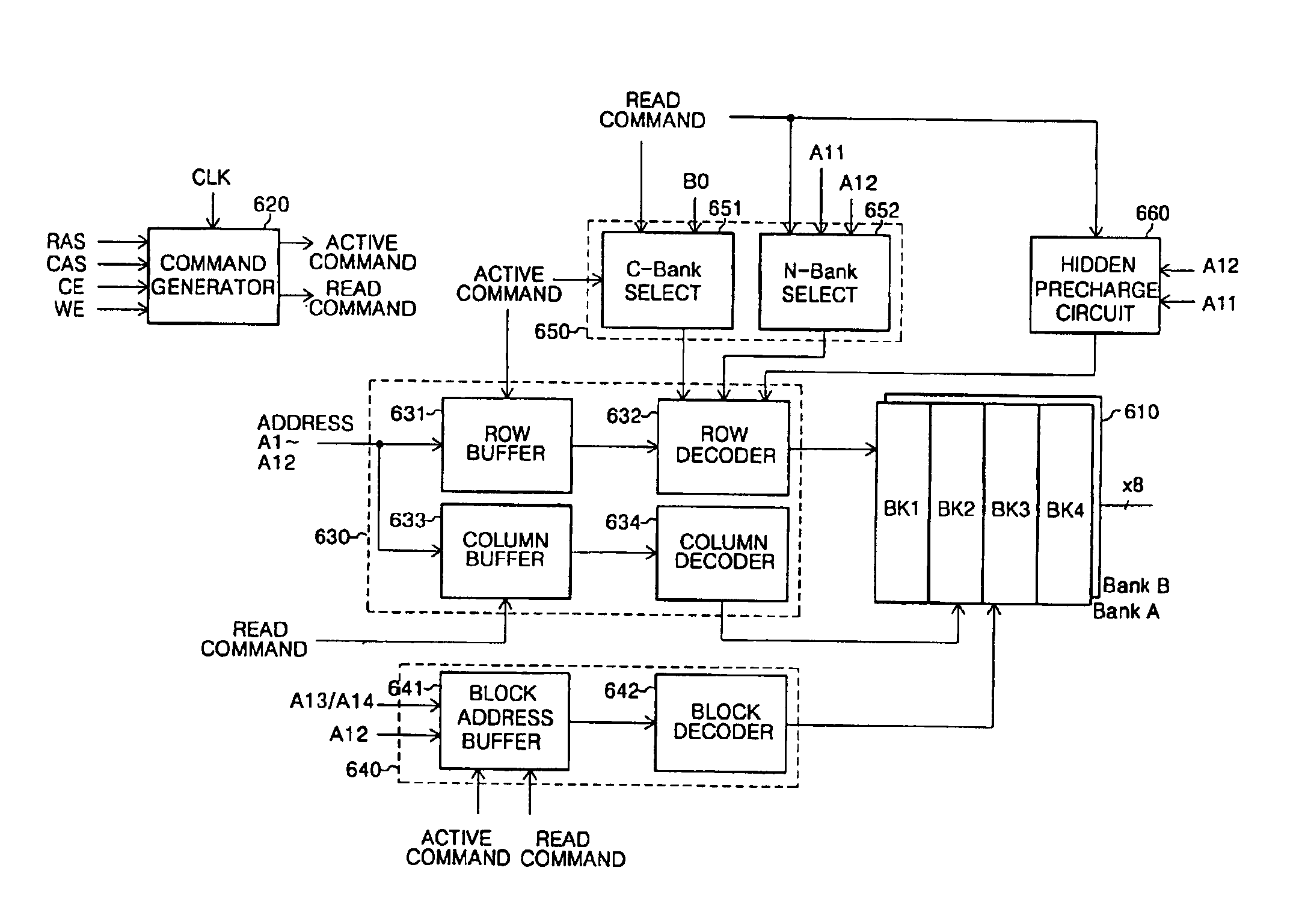
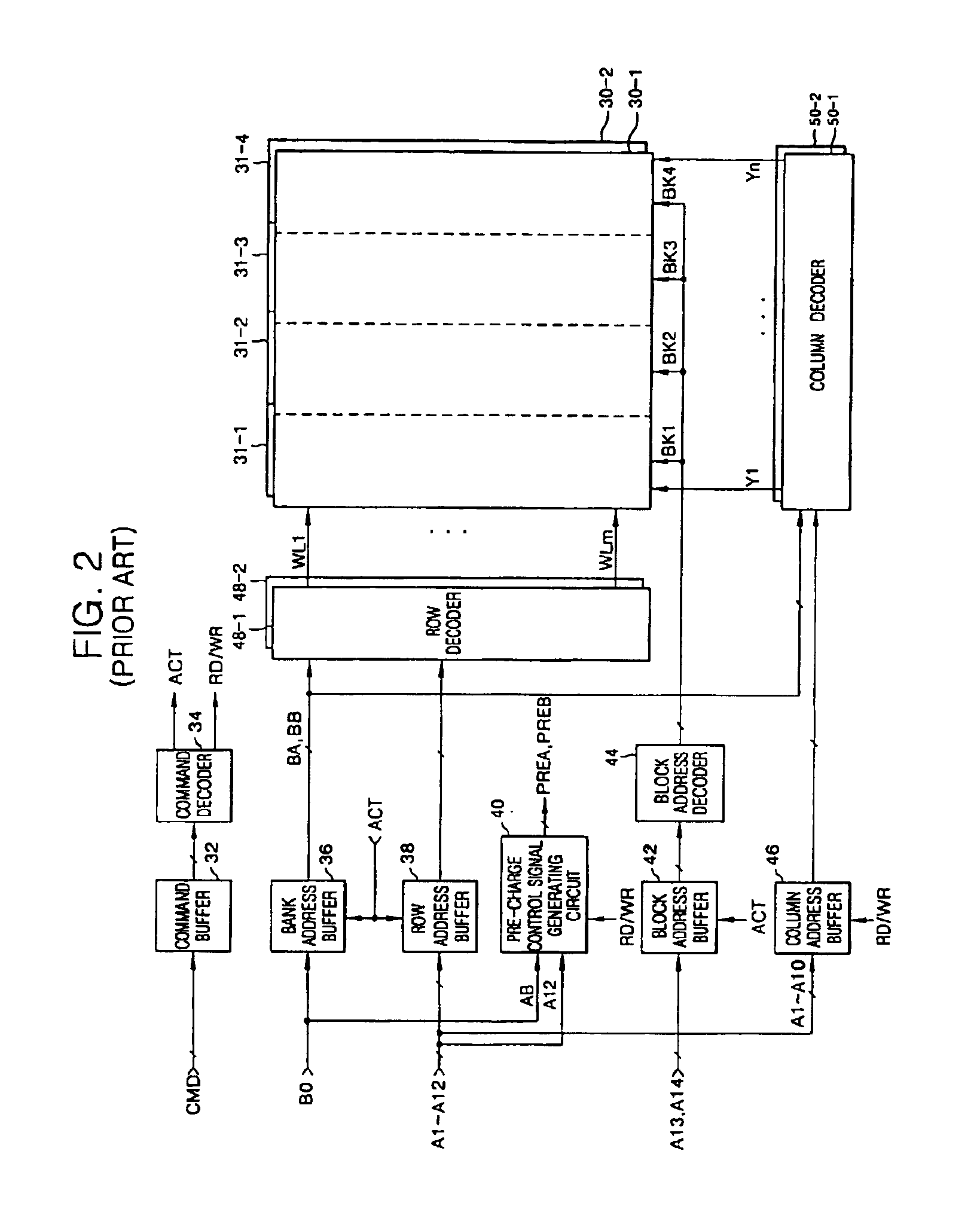
To fully understand the invention, the operational advantages thereof and the objects accomplished by the invention, preferred embodiments of the present invention will hereinafter be described with reference to the accompanying drawings. The same reference numerals in the respective drawings denote the same elements.

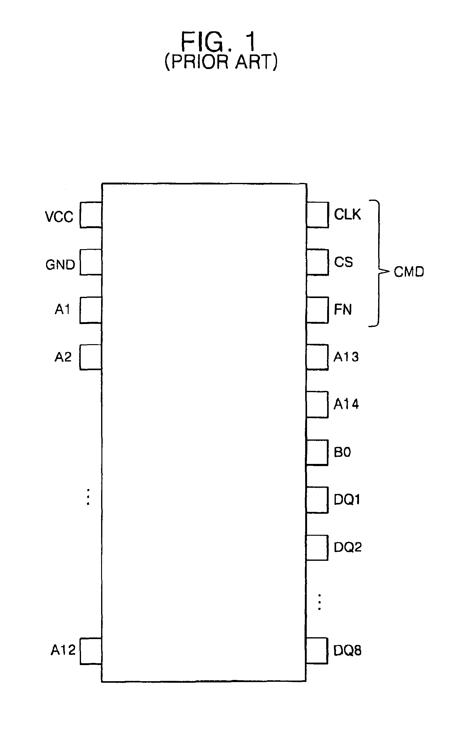
FIG. 5 shows a pin configuration of a 64 M-bit semiconductor memory device having two memory cell array banks and eight data I / O pins DQ1 to DQ8.

The semiconductor memory device of FIG. 5 includes a power voltage pin VCC, a ground pin GND, address pins A1 to A12, block address pins A13 and A14, a bank address pin B0, data I / O pins DQ1 to DQ8, and command pins CMD (RAS, CAS, CS and WE pin). The command pins CMD can be used to apply a system clock signal CLK, a row address strobe signal RASB, an column address strobe signal CASB, an chip selecting signal CSB, and an write enable signal WEB.

An ACTIVE command is issued by the assertion at logic high of the RASB signal on the...


PUM


Abstract

In a semiconductor memory device having a plurality of memory cells grouped in memory banks, each memory bank having a plurality of memory blocks accessible by a common row address, a method of reading from or writing to the plurality of memory blocks, comprising the steps of detecting successive read or write operations of different blocks, prefetching the address of the next block to be read or written during the first of the successive read or write operations; and withholding a precharge of the memory bank having the successively read or written memory blocks after the first of the successive read or write operations until completion of the successive read or write operations. A semiconductor memory device is also provided having a circuit for inhibiting the activation of the precharge signal at the end of a first memory access operation when successive memory access operations are to be performed with the first memory access operation at a first row address and a first memory block and the next memory access operation at the same first row address and a second memory block having a block address different from the first memory block.

Description

BACKGROUND OF THE INVENTION1. Technical FieldThe present invention is directed to a semiconductor memory device; in particular, a DRAM having a segmental cell array.2. Discussion of the Related ArtGenerally, a DRAM read / write operation involves three commands—an active command to select a row address and a word line, an RD / WR command (a read command or a write command) to select a bit line and a column address, and a precharge command to complete read / write operation and prepare a next read / write operation.To achieve high-speed data transfer rate, the recent trend in the DRAM industry has focused on improvements in interface performance, and generally not on any changes in the DRAM core. As a result, the memory access time tRC has not greatly improved, and effective bandwidth falls steeply when the row address changes frequently. The practice of dividing a memory array into multiple banks (multi-bank approach) may improve the performance somewhat, but the problem of address transiti...

Claims


Application Information

Patent Timeline
Patent Type & Authority Patents(United States)
IPC IPC(8): G11C7/12G11C7/00G11C7/22G11C11/4094G11C11/4076G11C11/409G11C11/407G11C11/401
CPCG11C7/12G11C7/22G11C11/4094G11C11/4076G11C2207/229G11C2207/2281G11C7/00
Inventor LEE, JAE-GOO
Owner SAMSUNG ELECTRONICS CO LTD
Why Eureka
Try Eureka