
Methods of creating patterns on substrates and articles of manufacture resulting therefrom

a technology of substrates and patterns, applied in the field of creating patterns on substrates, can solve the problems of insufficient robustness to be used as the barrier layer in dry etching, the geometry of ever shrinking devices has come to a bottleneck, and the need for high temperature and pressur

Inactive Publication Date: 2005-03-01
AGENCY FOR SCI TECH & RES +1
View PDF6 Cites 81 Cited by
  • Summary
  • Abstract
  • Description
  • Claims
  • Application Information

AI Technical Summary

Problems solved by technology

The ever shrinking device geometry has come to a bottleneck due to the limitation of the available lithography technology that is used to define the device minimum feature sizes.
The SAM patterns can be transferred to a substrate through special wet etching processes, but are not robust enough to be used as the barrier layer in dry etching.
Because significant polymer flow is required during NIL processes, very high temperature and pressure are needed.
However, because a polymer film continually covers a patterned mold after spin coating, the inked patterns usually display ragged edges due to forced breakage of the polymer film near feature sidewalls.
Very rough edges resulted, and the process can only be practiced with paste-like materials having very low cohesive strength.

Method used


Image

  • Methods of creating patterns on substrates and articles of manufacture resulting therefrom
  • Methods of creating patterns on substrates and articles of manufacture resulting therefrom
  • Methods of creating patterns on substrates and articles of manufacture resulting therefrom

Examples


example 1

FIG. 4 demonstrates the effect of selective surface treatment on polymer dewetting on a patterned mold. A 700 nanometer (run) period grating mold was spin coated with 4.5% poly(methyl methacrylate) (PMMA) (Mw=15,000 and Tg=105° C.) solution in toluene and then baked at 130° C. for 5 minutes. In FIG. 4(a), the mold was treated with FDTS solution alone. Because of the low surface energy of the FDTS treated surface, the PMMA film dewetted on the protruded surfaces and broke up into elongated droplets. In contrast, the mold in FIG. 4(b) was treated with selective PETS / FDTS as taught in accordance with the present invention. As the surface energy of the sidewalls was very low, the film dewetted near the edges of the protrusions. However, because of the higher surface energy of the PETS treated top surface of the protrusions, the film is continuous on the protrusions. The dewetted polymer lines were slightly narrower than the features on the mold. The polymer islands illustrated in FIG. 4...

example 2

FIG. 5 shows PMMA inking results with selective MOPTS / FDTS treatment. After spin coating and annealing, the PMMA film on the mold displayed an interesting feature as illustrated in the AFM scan in FIG. 5(a). A raised rim surrounded the PMMA island on top of the protrusions. Similar behavior is also observed on PETS / FDTS treated mold. The raised rim was likely formed by material retracting from the edge of the feature. During annealing, the thin polymer film on the sidewalls started to dewet first. The PMMA film retracted toward both the bottom of the trench and the protruded surface. Because of the higher energy of the protruded surfaces, the bulk of the PMMA film at the interface with the protrusions was immobilized. The retracted film piled up near the edge of the feature until the least interaction potential between PMMA and the surface is reached. Dewetting with this mechanism caused causes the film to shrink into a plateau surrounded with a rim and a pattern dimension change of...

example 3

For thin polycarbonate (PC, Lexan® ML6155-111N, Mw=18 k, Tg=150° C.) coatings on selective PETS / FDTS treated micrometer-sized molds, continuous PC film covers the 500 nm deep mold (FIG. 6(a)) after spin coating. When a relatively deep mold is used, however, isolated polymer islands are formed on the protrusions directly after spin coating. FIG. 6 compares the AFM scans of PC coated 500 mm and 720 nm deep molds. When a deep mold is coated with a polymer solution, the coating thickness on the sidewalls is likely to be very small. Spontaneous dewetting is then possible to occur on the sidewalls during spin coating, resulting in a discontinued coverage as shown in FIG. 6(b).

The polymer islands on protrusions continue to shrink during annealing until the equilibrium contact angle is reached, the resulted dimension change is around 60%. As a result, the inked features are usually much smaller than those on the mold. In fact, this offers a viable method to obtain submicrometer features usi...


PUM

PropertyMeasurementUnit
temperatureaaaaaaaaaa
thicknessaaaaaaaaaa
thicknessaaaaaaaaaa

Abstract

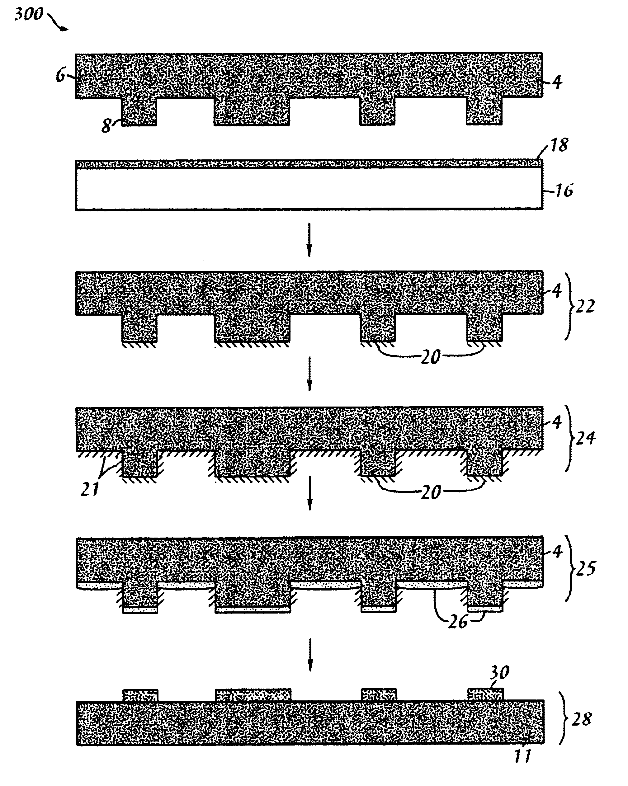
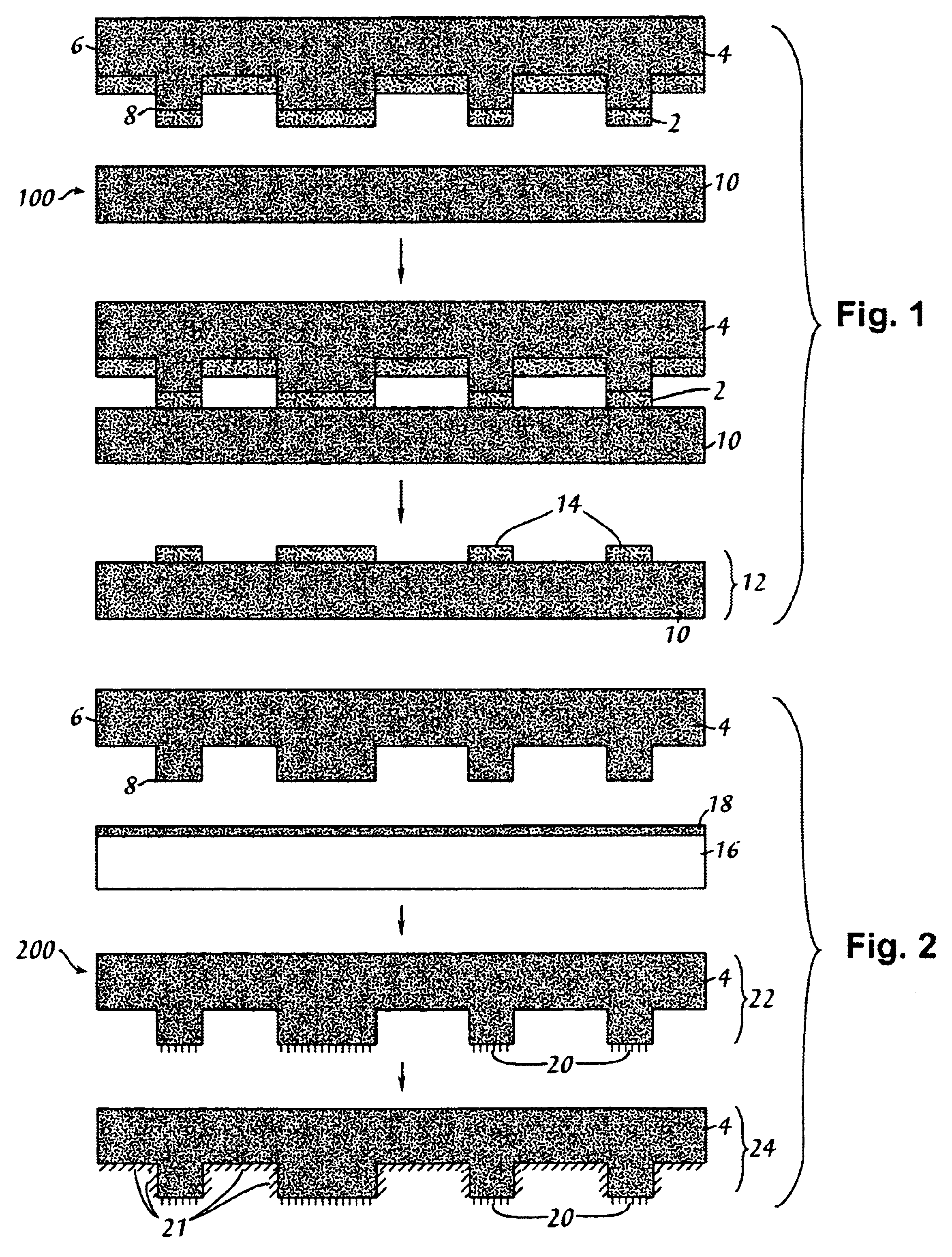
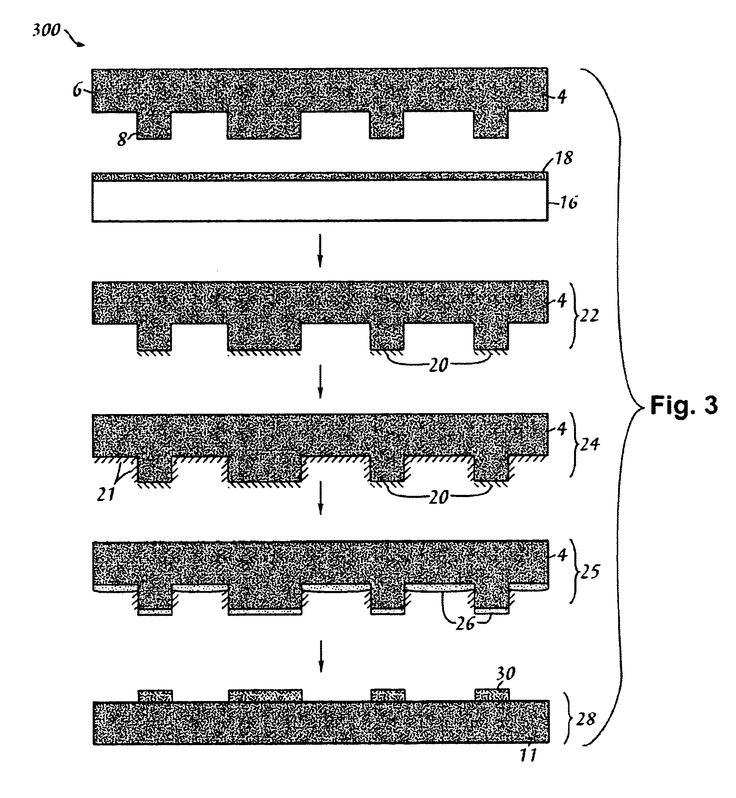
Methods of creating patterns on substrates are presented, and articles of manufacture resulting therefrom. One method comprises applying a first surface energy modifier to an applicator to form a coating on the applicator; contacting the coating with a receiving member, the receiving member having a topography, the coating only contacting and remaining on at least some protrusions; exposing the first modified receiving member to a second surface energy modifier, thereby forming a second modified receiving member having surface modified recesses; applying a composition comprising a polymeric material to the second modified receiving member, the composition substantially conforming to the topography of the surface modified protrusions and the surface modified recesses; and contacting the composition-coated, surface modified protrusions with a substrate for a time and under conditions sufficient to transfer the polymeric material on protrusions to the substrate. Because the surface energy of the sidewalls is lower than that on the protrusions, polymer dewetting from the sidewalls is promoted, which makes the polymer film discontinuous along the edges of patterns. Therefore, inked polymer patterns from the protrusions of the mold show very smooth edges and smaller dimensions compared to that of the mold.

Description

BACKGROUND INFORMATION1. Technical FieldThe invention is generally related to the field of creating patterns on substrates. More specifically, the invention relates to patterning substrates with polymeric materials having submicrometer-scale or nanometer-scale features.2. Background ArtThe trend in the semiconductor IC industry is to make devices smaller, faster and cheaper through very high degree of integration. The ever shrinking device geometry has come to a bottleneck due to the limitation of the available lithography technology that is used to define the device minimum feature sizes.In recent years a number of patterning techniques have been developed to overcome the resolution limit of photolithography. Among these newly developed methods, microcontact printing (μCP) and nanoimprint lithography (NIL) are two high throughput and low cost patterning techniques. Microcontact printing (μCP) typically utilizes a soft polydimethylsiloxane (PDMS) mold or stamp to print self-assemble...

Claims


Application Information

Patent Timeline
Patent Type & Authority Patents(United States)
IPC IPC(8): B05D3/10B29C33/00B44C1/165B44C3/00B44C3/08C03C17/28C03C17/30G03FG03F7/00
CPCB82Y10/00G03F7/0002B82Y40/00B82Y30/00
Inventor BAO, LIRONGTAN, LIHUANG, XUDONGKONG, YEN PENGGUO, LINGJIE JAYPANG, STELLA W.YEE, ALBERT
Owner AGENCY FOR SCI TECH & RES
Learn More