
Laser diode optical transmitter for TDMA system with fast enable and disable times

a laser diode and optical transmitter technology, applied in the field of optical transmitters, can solve the problems of increasing background noise, reducing the overall bandwidth of the pon for data transmission, etc., and achieve the effect of fast enable and disable of the laser diode, reducing the effect of parasitic capacitance, and high impedan

Inactive Publication Date: 2005-02-22
NORTHPEAK ENTERPRISES
View PDF8 Cites 12 Cited by
  • Summary
  • Abstract
  • Description
  • Claims
  • Application Information

AI Technical Summary

Benefits of technology

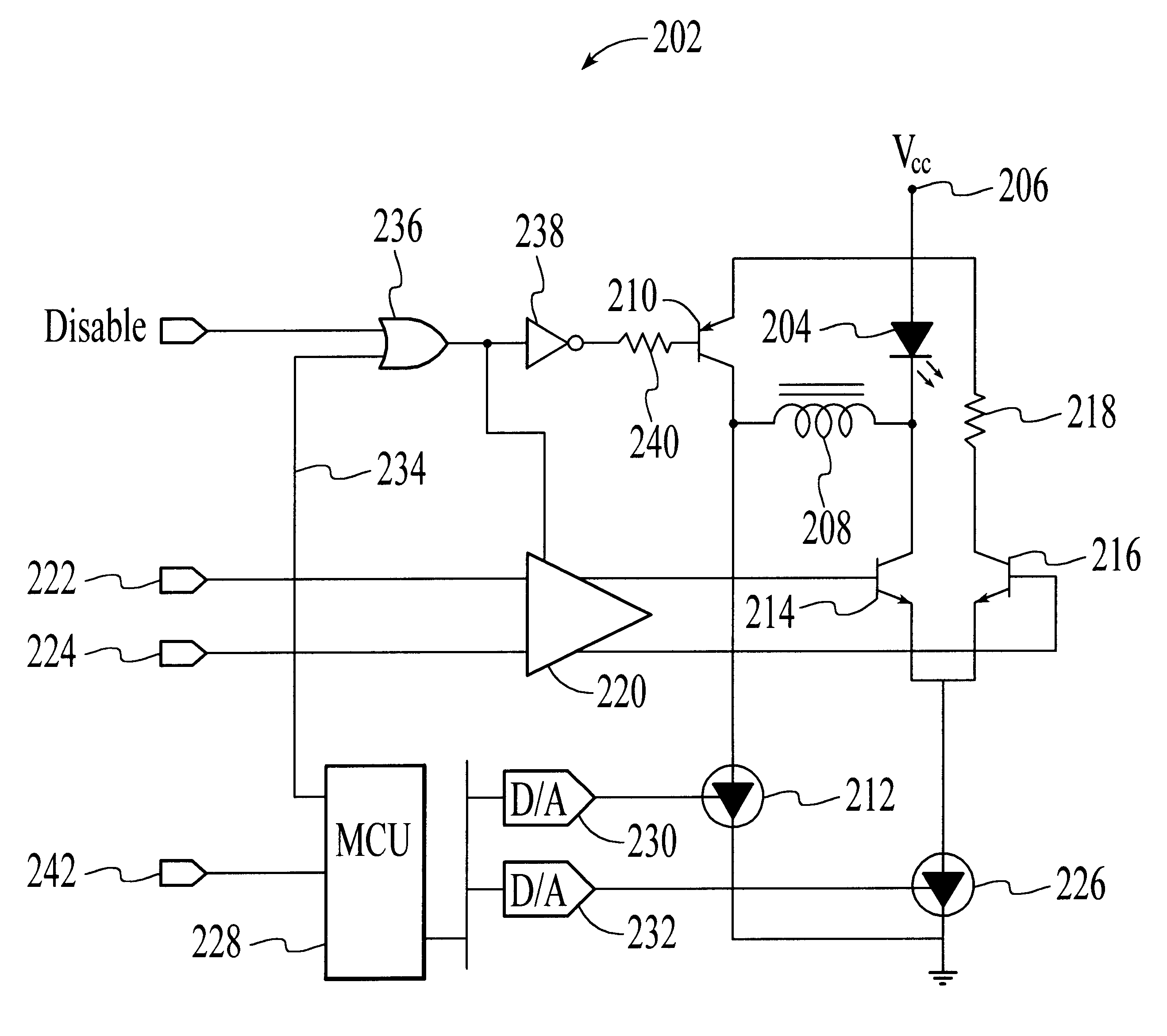
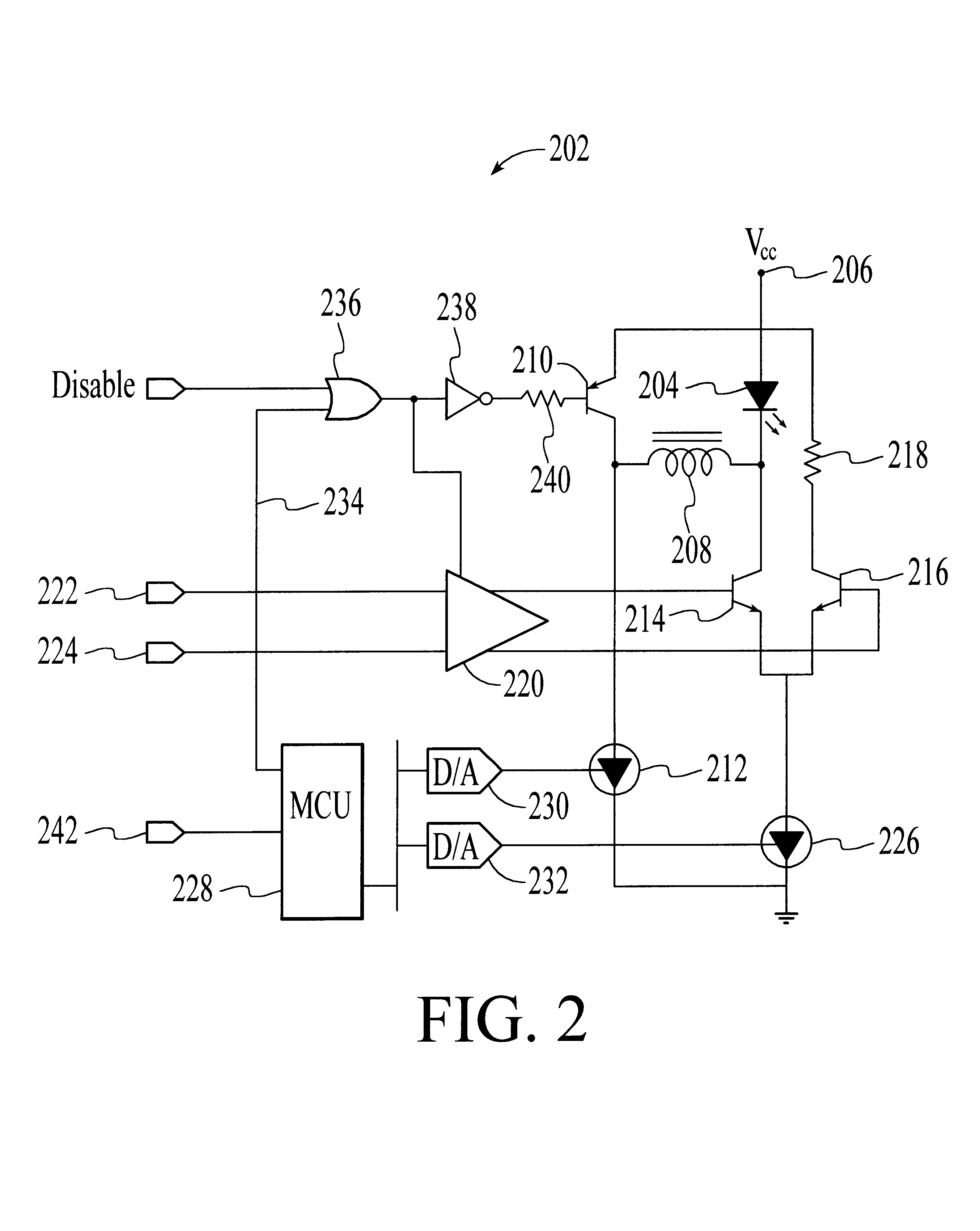
A laser diode optical transmitter and a method of operating the optical transmitter utilize a transistor to quickly enable and disable a laser diode by selectively shorting the laser diode. In an embodiment, the transistor is separated from the laser diode by an inductor. The inductor provides a high impedance between the transistor and the laser diode to at least reduce the effect of a parasitic capacitance associated with the transistor when the laser diode is driven to generate optical signals of different power levels. The use of the transistor and the inductor (i) reduces the amount of leakage light generated by the laser diode when in a disabled state, (ii) shortens the enable and disable times of the optical transmitter, and (iii) allows the laser diode to be modulated at a high rate of speed.
In an exemplary embodiment, the optical transmitter includes a light emitting device, a switching device, a modulation circuit and an inductive element. The light emitting device may be a laser diode that can generate light of different optical power levels. The switching device may be a transistor that is connected in parallel to the light emitting device to selectively short the light emitting device to disable the optical transmitter. In an embodiment, the transistor is a PNP bipolar transistor. The modulation circuit is configured to drive the light emitting device to generate light of different optical power levels. In an embodiment, the modulation circuit include a pair of differential transistors that are connected to the light emitting device and a modulation current source. The inductive element of the optical transmitter may be an inductor that provides an impedance between the light emitting device and the switching device. The impedance provided by the inductive element to at least reduce the effect of parasitic capacitance associated with the switching element when the light emitting device is driven by the modulation circuit.
In an exemplary embodiment, the method of operating an optical transmitter includes a step of driving a light emitting device to generate optical signals of different power levels and a step of providing an inductive impedance between the light emitting device and at least a switching device that can electrically short the light emitting diode. The inductive impedance reduces at least the effect of parasitic capacitance associated with the switching device when the light emitting device is driven to generate the optical signals. In an embodiment, the method also includes a step of receiving an indicator that is associated with a predefined condition to disable the optical transmitter and a step disabling the optical transmitter by activating the switching device to short the light emitting device in response to the indicator. In one embodiment, the step of receiving the indicator includes not receiving a patterned signal from an external source.

Problems solved by technology

However, the guard bands can occupy a significant amount of bandwidth and consequently, reduce the overall bandwidth of the PON for data transmission.
Any leakage of light from a single disabled optical transmitter may increase the background noise.
The overall effect is that significant background noise may be created by the combined light leakage, which may affect the OLT from differentiating legitimate data from the background noise.

Method used


Image

  • Laser diode optical transmitter for TDMA system with fast enable and disable times
  • Laser diode optical transmitter for TDMA system with fast enable and disable times
  • Laser diode optical transmitter for TDMA system with fast enable and disable times

Examples


Embodiment Construction

With reference to FIG. 2, a laser diode optical transmitter 202 for use in a passive optical network (PON) system that utilizes time division multiplex access (TDMA) is shown. The optical transmitter is characterized by fast enable and disable times so that the length of the guard bands used by the system can be minimized. In addition, the optical transmitter is designed to prevent, or significantly reduce, light leakage when disabled. Furthermore, the optical transmitter is designed to modulate output optical signals with sufficient speed for data transmission in the Gigabit per second range.

The optical transmitter 202 includes a laser diode 204 that is driven to emit binary optical signals. As illustrated in FIG. 3, the laser diode can be driven to generate light signals having an optical power level of P1, which are optical representations of “1” signals. Alternatively, the laser diode can be driven to generate light signals having an optical power level of P0, which are optical ...


PUM


Abstract

A laser diode optical transmitter and a method of operating the optical transmitter utilize a transistor to quickly enable and disable a laser diode by selectively shorting the laser diode. In an embodiment, the transistor is separated from the laser diode by an inductor. The inductor provides a high impedance between the transistor and the laser diode to at least reduce the effect of a parasitic capacitance associated with the transistor when the laser diode is driven to generate optical signals of different power levels. The use of the transistor and the inductor (i) reduces the amount of leakage light generated by the laser diode when in a disabled state, (ii) shortens the enable and disable times of the optical transmitter, and (iii) allows the laser diode to be modulated at a high rate of speed.

Description

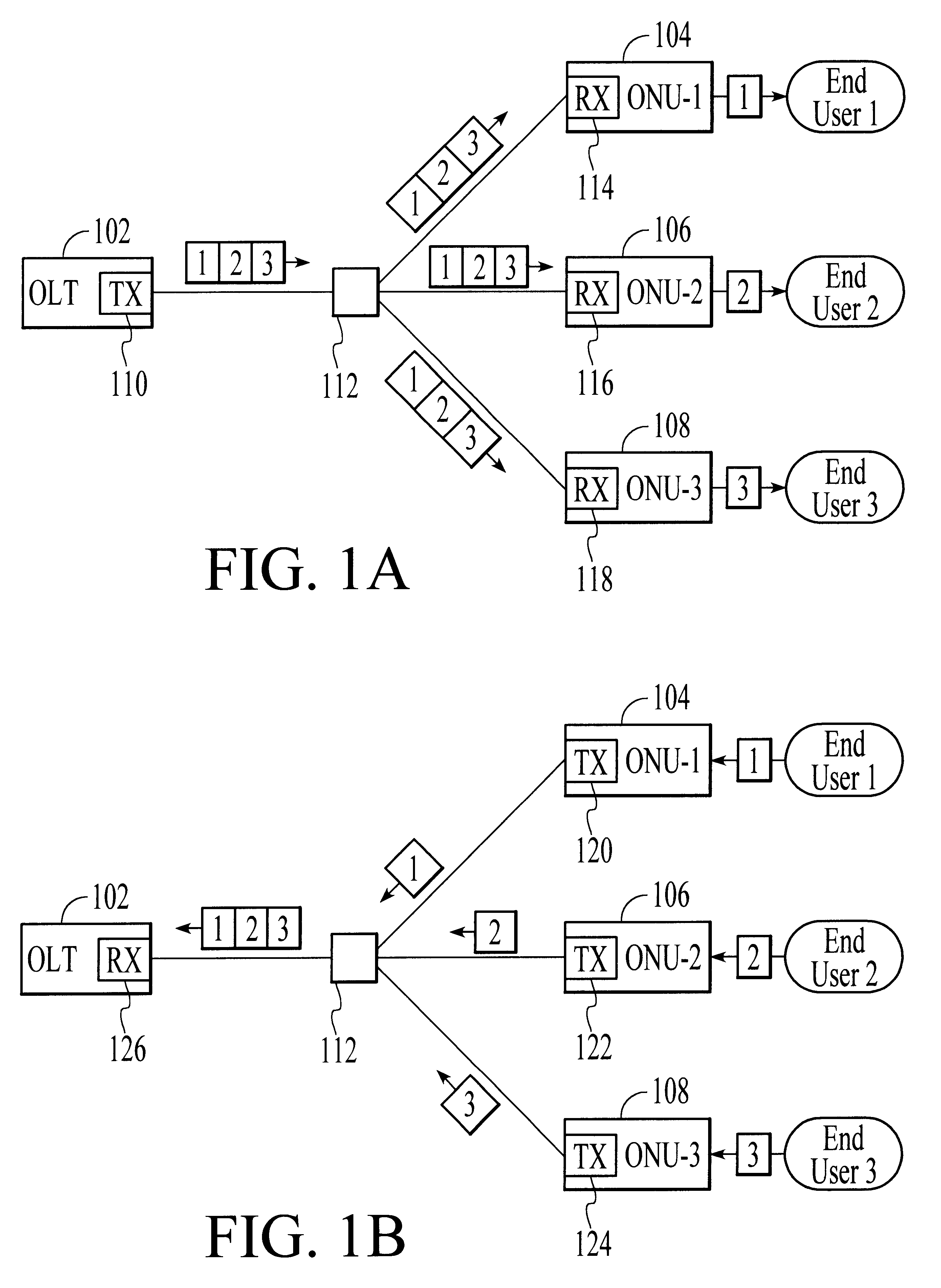
FIELD OF THE INVENTIONThe invention relates generally to optical transmitters, and more particularly to an optical transmitter for a time division multiplex access (TDMA) system.BACKGROUND OF THE INVENTIONThe explosion of the Internet and the desire to provide multiple communications and entertainment services to end users have created a need for a broadband network architecture that improves access to end users. One broadband network architecture that improves access to end users is a point-to-multipoint passive optical network (PON). A point-to-multipoint PON is an optical access network architecture that facilitates broadband communications between an optical line terminal (OLT) and multiple remote optical network units (ONUs) over a purely passive optical distribution network. A point-to-multipoint PON utilizes passive fiber optic splitters and couplers to passively distribute optical signals between the OLT and the remote ONUs.FIGS. 1A and 1B illustrate the management of networ...

Claims


Application Information

Patent Timeline
Patent Type & Authority Patents(United States)
IPC IPC(8): H04B10/155H04B10/152
CPCH04B10/508
Inventor KUO, JERCHENO'BRIEN, MICHAEL ANTHONY
Owner NORTHPEAK ENTERPRISES
Learn More