Cutting CAM peak power by clock regioning

a clock region and cam technology, applied in the field of cam peak power reduction, can solve the problems of cam device b>200/b> having a peak power consumption which may be significantly higher, cam device b>200/b> having a significantly higher peak power consumption, etc., and achieve the effect of reducing the peak power consumption of the cam devi

Inactive Publication Date: 2005-02-15
MICRON TECH INC
View PDF3 Cites 29 Cited by
  • Summary
  • Abstract
  • Description
  • Claims
  • Application Information

AI Technical Summary

Benefits of technology

The invention provides a CAM device architecture where the CAM cells are divided into at least two arrays. Each array is operated in a different clock domain so that each array is prevented from drawing maximum power at a same time. By dividing the CAM array into a plurality of arrays and staggering the search operation so that every array does not simultaneously draw maximum power, the peak power consumption of the CAM device is reduced.

Problems solved by technology

However, CAM devices 200 consume significantly more power and produce significantly more switching noise than a conventional memory device, especially during a first portion of the search operation because the CAM cells 100 are accessed and searched simultaneously.
This results in the CAM device 200 having a peak power consumption which may be significantly higher than the average power consumption during a portion of each match operation.
The high peak power consumption requires the CAM device 200 to be used with a robust power supply, and also increases heat production.

Method used


Image

  • Cutting CAM peak power by clock regioning
  • Cutting CAM peak power by clock regioning
  • Cutting CAM peak power by clock regioning

Examples


second embodiment

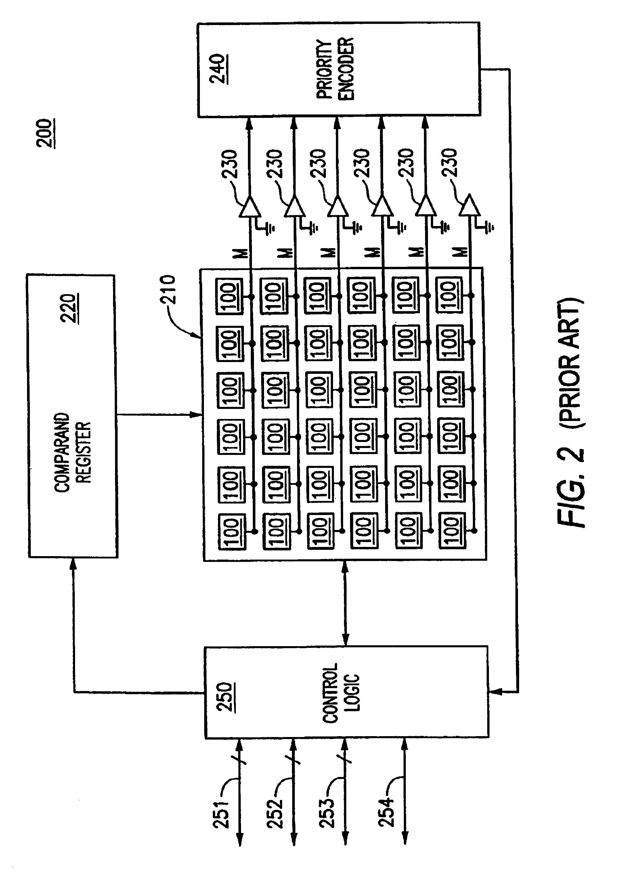
The second embodiment differs more from the first embodiment subsequent to clock cycles 5 and 5′, due to the changes in the number of, and operation of, the priority encoders. As a result, the timing diagram of FIG. 4B omits cycles 1-5 and 1′-5′ and spans only clock cycles 6-10 and 6′-10′. The processing which occurs during these cycles is now explained:

In clock cycle 6, priority encoders 240a1 and 240a2 each output their results to priority encoder 240a3. In clock cycle 6′, priority encoders 240b1 and 240b2 output their results to priority encoder 240b3. In clock cycle 7, priority encoder 240a3 outputs its result to priority encoder 240c. In clock cycle 7′, priority encoder 240b3 outputs its result to priority encoder 240c. No task is associated with clock cycle 8. In clock cycle 8′, priority encoder 240c outputs it result to control circuit 250″. In clock cycle 9, the control circuit 250″ outputs the final result of the search process (off-chip). No task is associated with clock c...


PUM


Abstract

A CAM device architecture where CAM cells are divided into at least two arrays and each array is operated in a different clock domain so that at no time are the arrays simultaneously drawing maximum power. By dividing the CAM array into a plurality of arrays and staggering the search operation so that every array does not simultaneously draw maximum power, the peak power consumption of the CAM device is reduced.

Description

FIELD OF INVENTIONThe present invention relates generally to semiconductor memory devices and, more particularly to peak power reduction in content addressable memory (CAM) devices.BACKGROUND OF THE INVENTIONAn essential semiconductor device is semiconductor memory, such as a random access memory (RAM) device. A RAM allows a memory circuit to execute both read and write operations on its memory cells. Typical examples of RAM devices include dynamic random access memory (DRAM) and static random access memory (SRAM).Another form of memory is the content addressable memory (CAM) device. A CAM is a memory device that accelerates any application requiring fast searches of a database, list, or pattern, such as in database machines, image or voice recognition, or computer and communication networks. CAMs provide benefits over other memory search algorithms by simultaneously comparing the desired information (i.e., data in the comparand register) against the entire list of pre-stored entrie...

Claims


Application Information

Patent Timeline
Patent Type & Authority Patents(United States)
IPC IPC(8): G11C15/00
CPCG11C15/00
Inventor RADKE, WILLIAM
Owner MICRON TECH INC
Why Eureka
Try Eureka