Methods for fabricating semiconductor devices

a technology of semiconductor devices and manufacturing methods, applied in the direction of semiconductor devices, electrical appliances, transistors, etc., can solve the problems of reducing the yield of semiconductor devices, affecting the performance of semiconductor devices, and affecting the efficiency of semiconductor devices, so as to prevent an incidence of attack or erosion

Inactive Publication Date: 2005-02-08
SK HYNIX INC
View PDF5 Cites 12 Cited by
  • Summary
  • Abstract
  • Description
  • Claims
  • Application Information

AI Technical Summary

Benefits of technology

Methods for fabricating semiconductor devices are disclosed which are capable of preventing an incidence of attack or erosion to bottom layers during wet-type etching performed in the course of a storage node contact formation.
A disclosed method for fabricating a semiconductor device comprises forming a plurality of first plugs in contact with a substrate that passes through a first inter-layer insulation layer; forming a second inter-layer insulation layer on the first plugs; forming a conductive pattern in contact with a group of the first plugs by etching selectively through the second inter-layer insulation layer; and forming a contact hole that exposes a surface of the first plug that is not in contact with the conductive pattern by etching selectively through the second insulation layer with a dry-type and wet-type etch process, wherein an attack barrier layer is formed between the first inter-layer insulation layer and the second inter-layer insulation layer to prevent an incidence of attack or erosion of the first interlayer insulation layer in contact with the first plug during the wet-type etch process for forming the contact hole.

Problems solved by technology

The erosion 26 can induce an electric short with the storage node, bit line or other conductive wires, thereby deteriorating performances of the semiconductor device.
This void effect becomes a critical factor that gives rise to an electric short between the electrodes and reduces yields of the semiconductor devices.
However, this technique is practically impossible due to difficulties in obtaining sufficient spaces for isolating each device and in applying the SAC process.
Furthermore, it is difficult to increase the width of the bit line in practice due to difficulties in obtaining a CD of the bottom side of the contact and a deterioration of the gap-fill properties during the storage node contact formation process.

Method used


Image

  • Methods for fabricating semiconductor devices
  • Methods for fabricating semiconductor devices
  • Methods for fabricating semiconductor devices

Examples


first embodiment

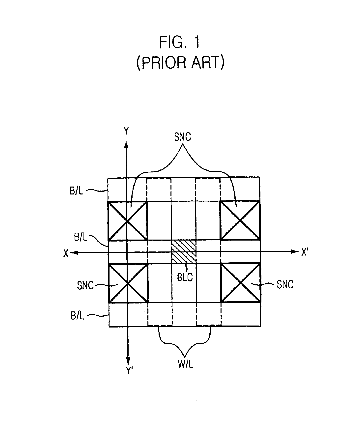
With reference to FIGS. 2A to 2B and FIGS. 4A to 4D, a method for fabricating a semiconductor device is disclosed in accordance with a FIGS. 2A to 2B are cross-sectional views taken along lines X-X′ and Y-Y′ shown of FIG. 1 after successive steps of the disclosed process.

Referring to FIG. 2A, a gate electrode 11 is formed on a substrate 10 containing various elements of the semiconductor device. In greater detail, the gate electrode 11 is formed with a single or stack layer of tungsten or polysilicon. A gate insulation layer (not shown) is formed at an interface between the gate electrode 11 and the substrate 10. On top of the gate electrode 11, a nitride- based hard mask (not shown) is formed from an oxide-based inter-layer insulation layer to protect the gate electrode 11 during a self align contact (SAC) process and to obtain an appropriate etch profile during the SAC process. The hard mask has a different etch selectivity than that gate electrode 11.

At this time, in 0.1 μm or b...

second embodiment

FIGS. 5A to 5E are cross-sectional views of a semiconductor device made in accordance with a

For the sake of simplicity, FIG. 1 and FIG. 2A of the prior art are used in the drawings for the second preferred embodiment of the present invention, and those constitutional elements of the second preferred embodiment identical to the prior art are denoted using the same reference numerals.

Referring to FIG. 2A, a gate electrode 11 is formed on a substrate 10 containing various elements of a semiconductor device. An active region (not shown) is then formed by performing an ion implantation technique to a portion of the substrate 10 allocated between the gate electrodes 11.

Referring to FIG. 5A, a first inter-layer insulation layer 12 of which top is planarized is formed. Continuous to the formation of the first inter-layer insulation layer 12, an attack barrier layer 30 is formed thereon. The attack barrier layer 30 is for preventing the attack to the first inter-layer insulation layer 12 alo...


PUM


Abstract

A method for fabricating a semiconductor device includes forming a plurality of first plugs contacted to a substrate by passing through a first inter-layer insulation layer; forming a second inter-layer insulation layer on the first plugs; forming a conductive pattern contacted to a group of the first plugs by etching selectively the second inter-layer insulation layer; and forming a contact hole exposing a surface of the first plug that is not contacted to the conductive pattern by etching selectively the second insulation layer with use of a dry-type and wet-type etch process, wherein an attack barrier layer is formed on between the first inter-layer insulation layer and the second inter-layer insulation layer to thereby prevent an incidence of attack to the first interlayer insulation layer contacted to the first plug during the wet-type etch process for forming the contact hole.

Description

BACKGROUND1. Technical FieldA method for fabricating a semiconductor device is disclosed and, more particularly, a method for fabricating a semiconductor device that prevents degradation of the semiconductor device caused by damage to an insulation layer during a process for forming an opening for a storage node contact.2. Description of the Related ArtThere have been numerous attempts at achieving higher integration and higher performance of semiconductor devices. With respect to the higher integration, it is essential to develop technologies for obtaining contact regions as well as for enhancing gap-filled properties.FIG. 1 is a plan view schematically illustrating a conductive pattern including a word line for forming a bit line and the bit line. In FIG. 1, a plurality of gate electrodes, e.g., word lines W / L, are aligned in one direction, and a plurality of bit lines B / L are aligned in another direction to thereby cross or intersect the word lines W / L. A plurality of landing plu...

Claims


Application Information

Patent Timeline
Patent Type & Authority Patents(United States)
IPC IPC(8): H01L21/02H01L21/70H01L21/768H01L21/311H01L21/306H01L21/308H01L21/8242H01L27/108
CPCH01L21/31111H01L21/31116H01L21/76802H01L21/76829H01L27/10855H01L21/76804H01L27/10885H01L27/10814H10B12/315H10B12/0335H10B12/482
Inventor LEE, SUNG-KWONLEE, MIN-SUKKIM, SANG-IK
Owner SK HYNIX INC
Why Eureka
Try Eureka