Non-volatile semiconductor memory device with NAND string memory transistor controlled as block separation transistor

a non-volatile, semiconductor technology, applied in transistors, digital storage, instruments, etc., can solve the problems of reducing usability, shrinking of gate transistors and contact portions, and increasing the size of the unit of data erasur

Active Publication Date: 2005-02-01
KIOXIA CORP
View PDF5 Cites 92 Cited by
  • Summary
  • Abstract
  • Description
  • Claims
  • Application Information

AI Technical Summary

Benefits of technology

According to one aspect of the present invention, there is provided a non-volatile semiconductor memory device including:a memory cell array having NAND strings arranged therein, each NAND string having a plurality of electrically rewritable and non-volatile memory transistors connected in series; andan erase / write / read control circuit configured to perform erasing, writing and reading of the memory cell array, whereinat least one memory transistor within each NAND string of the memory cell array is controlled as a block separation transistor for dividing the memory cell array into a plurality of blocks each serving as a unit of data erasure.

Problems solved by technology

Although NAND flash memories are capable of lessening the size of a NAND string per se by reducing a minimum device feature size, it is unlikely that select gate transistors and contact portions are shrinkable in a way simply proportional to their microfabrication sizes.
On the other hand, when an attempt is made to maintain the high integration density of a flash memory by increasing the number of those memory cells making up a NAND string, the unit of data erasure becomes larger, resulting in a decrease in usability.
This in turn causes a problem that the number of data rewrite is limited.

Method used


Image

  • Non-volatile semiconductor memory device with NAND string memory transistor controlled as block separation transistor
  • Non-volatile semiconductor memory device with NAND string memory transistor controlled as block separation transistor
  • Non-volatile semiconductor memory device with NAND string memory transistor controlled as block separation transistor

Examples


Embodiment Construction

Embodiments of this invention will be set forth with reference to the accompanying drawings below.

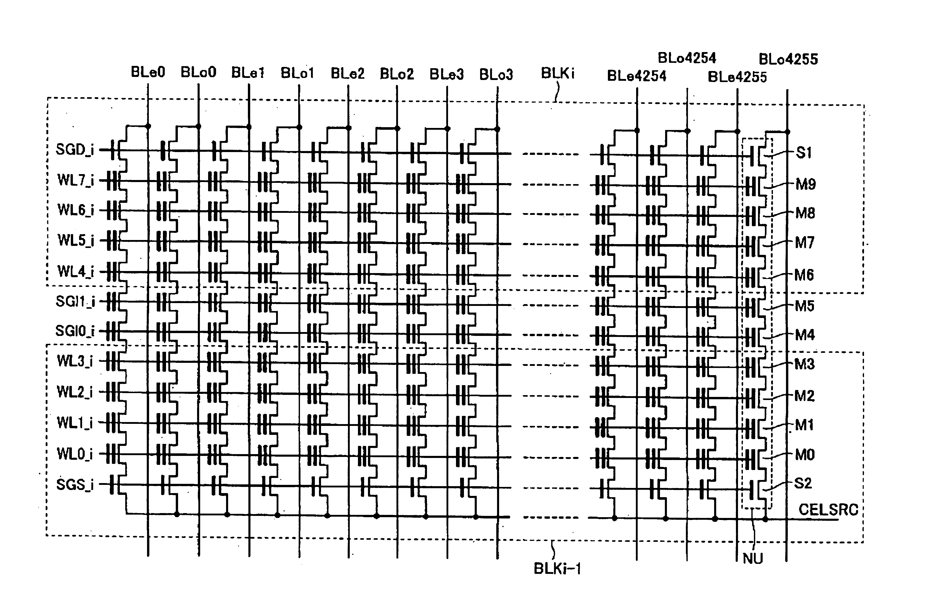
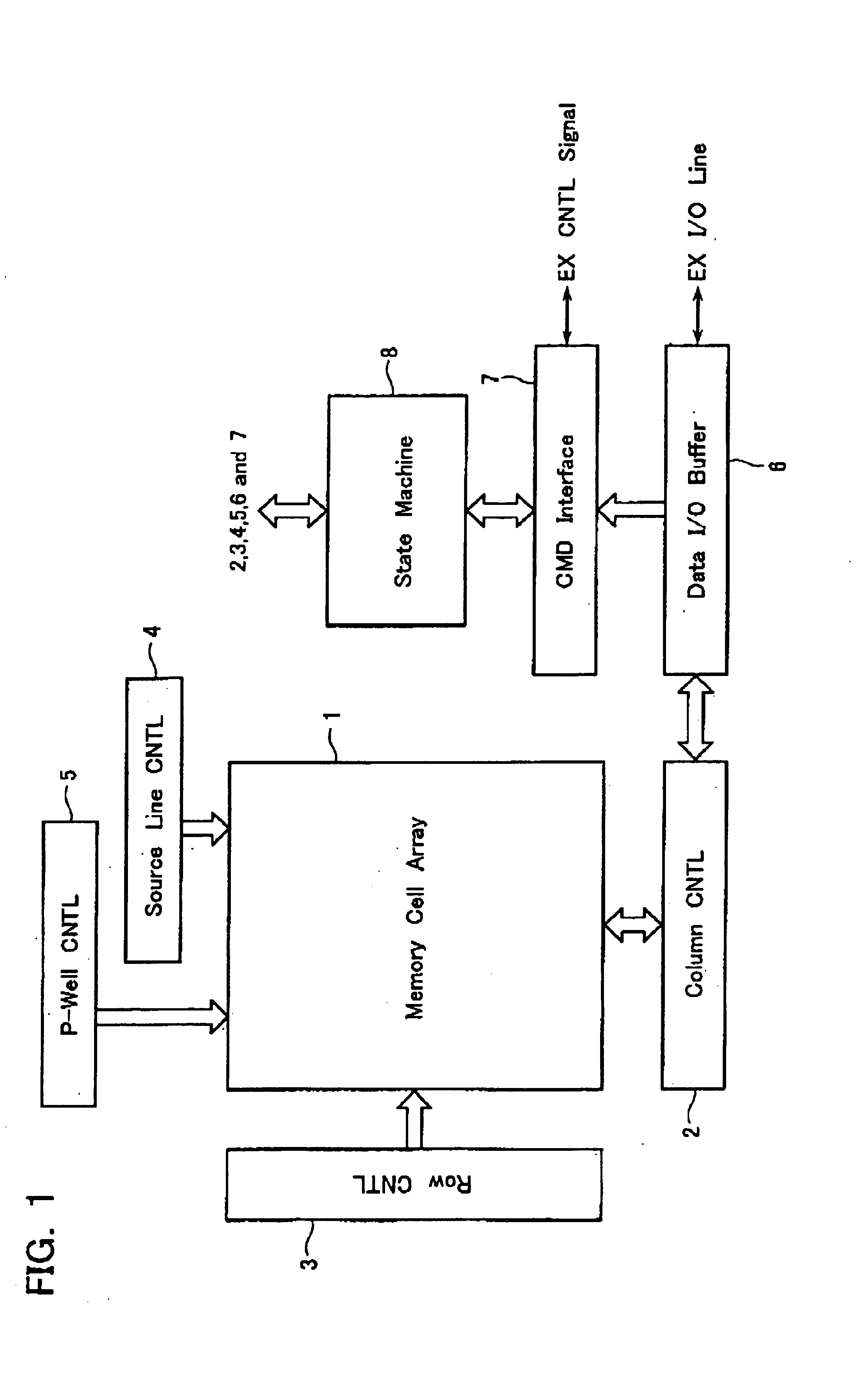
FIG. 1 illustrates, in functional block diagram form, a configuration of a flash EEPROM chip of the NAND type in accordance with one embodiment of the invention. The NAND flash memory includes a memory cell array 1, which is generally configured from a matrix of rows and columns of electrically rewritable or “reprogrammable” nonvolatile memory transistors (memory cells). The memory cell array 1 is operatively associated with a column control circuit 2 which is provided adjacent thereto. This column control circuit 2 is for control of bit lines of the memory cell array 1 to thereby perform data erasure of a memory cell(s), data write into a memory cell(s), and data read out of a memory cell(s). The column control circuit 2 has a sense amplifier circuit for reading cell data, a data latch circuit for retaining read and write data, and column select gates.

A row control circuit 3 is provide...


PUM


Abstract

A non-volatile semiconductor memory device includes: a memory cell array having NAND strings arranged therein, each NAND string having a plurality of electrically rewritable and non-volatile memory transistors connected in series; and an erase/write/read control circuit configured to perform erasing, writing and reading of the memory cell array, wherein at least one memory transistor within each NAND string of the memory cell array is controlled as a block separation transistor for dividing the memory cell array into a plurality of blocks each serving as a unit of data erasure.

Description

CROSS-REFERENCE TO PRIOR APPLICATIONThis application is based upon and claims the benefit of priority from the prior Japanese Patent Application No. 2003-351893, filed on Oct. 10, 2003, the entire contents of which are incorporated herein by reference.BACKGROUND OF THE INVENTION1. Field of the InventionThe present invention relates generally to an electrically rewritable non-volatile semiconductor memory device such as electrically erasable programmable read only memory (EEPROM). More particularly but not exclusively, this invention relates to a “flash” memory of a NAND type.2. Description of Related ArtFlash memories are designed to store as data different threshold voltage states of a memory cell (memory transistor) in a way pursuant to the amount of electrical charge of a floating gate thereof. For example, a flash memory stores a negative threshold state as a bit of logic “1” data and stores a positive threshold state as a logic “0” data bit. Data rewriting (erasure and write), ...

Claims


Application Information

Patent Timeline
Patent Type & Authority Patents(United States)
IPC IPC(8): G11C16/02G11C16/16G11C16/04G11C16/06H01L29/66H01L27/115H01L21/70H01L21/8247H01L27/10H01L29/792H01L29/788G11C16/00
CPCG11C16/16G11C16/0483G11C16/00
Inventor TANAKA, TOMOHARU
Owner KIOXIA CORP
Why Eureka
Try Eureka