Miniaturized multi-layer coplanar wave guide low pass filter

Active Publication Date: 2005-01-25
CYNTEC
View PDF6 Cites 9 Cited by
  • Summary
  • Abstract
  • Description
  • Claims
  • Application Information

AI Technical Summary

Benefits of technology

Accordingly, it is a first object of the present invention to provide a low pass filter which can greatly reduce the area occupied by the filter so as to fulfill the current radio communication system's needs of light, thin, short, and small structure.
It is a second object of the present invention that the provided low pass filter is a miniaturized multi-layer coplanar wave guide low pass filter whose metallic parts, substrate material, and dielectric material are all incorporated to greatly enlarge the region of its characteristic impedance.
It is a third object of the present invention to provide a miniaturized multi-layer coplanar low pass filter which can be fabricated by thin film fabrication technology therefore not only capable of achieving the product compactness but also greatly reducing the time and cost for production so as to strengthen the competitive ability in the market.

Problems solved by technology

The above mentioned via holes tend to bring about innegligible inductance effect at high frequency resulting in reducing efficiency of the circuit.
However, it is found to be impracticable as the area occupied by these circuits is considerably large.
In the meanwhile, it is found the area of this two-dimensional coplanar wave guide low pass filter is still unable to be reduced to a satisfactory extent which complies with the compactness of light, thin, short, and small that fulfils the current radio communication system's needs.
In addition, the conventional coplanar wave guide filter has a characteristic impedance in the range of 50˜70Ω which is considered one of the disadvantages when it is to be in match with the network.

Method used


Image

  • Miniaturized multi-layer coplanar wave guide low pass filter
  • Miniaturized multi-layer coplanar wave guide low pass filter
  • Miniaturized multi-layer coplanar wave guide low pass filter

Examples


Embodiment Construction

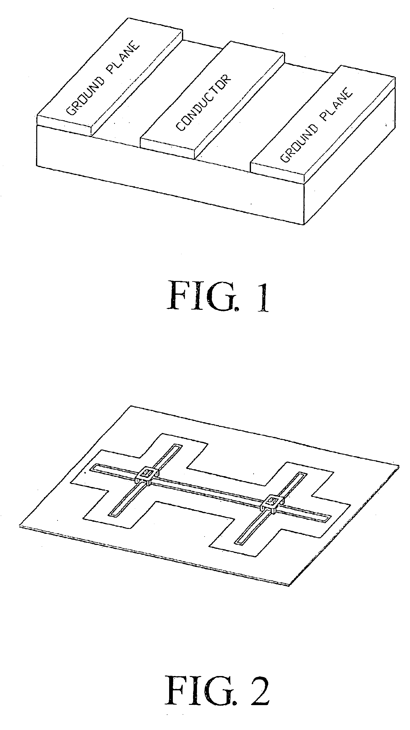
The structure and shortcomings of the conventional two-dimensional coplanar wave guide low pass filter have already been illustrated above therefore will not be described herein again.

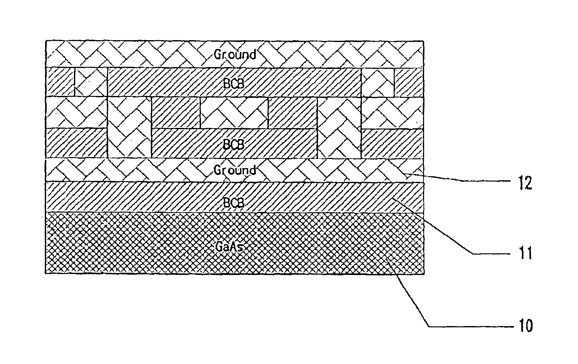
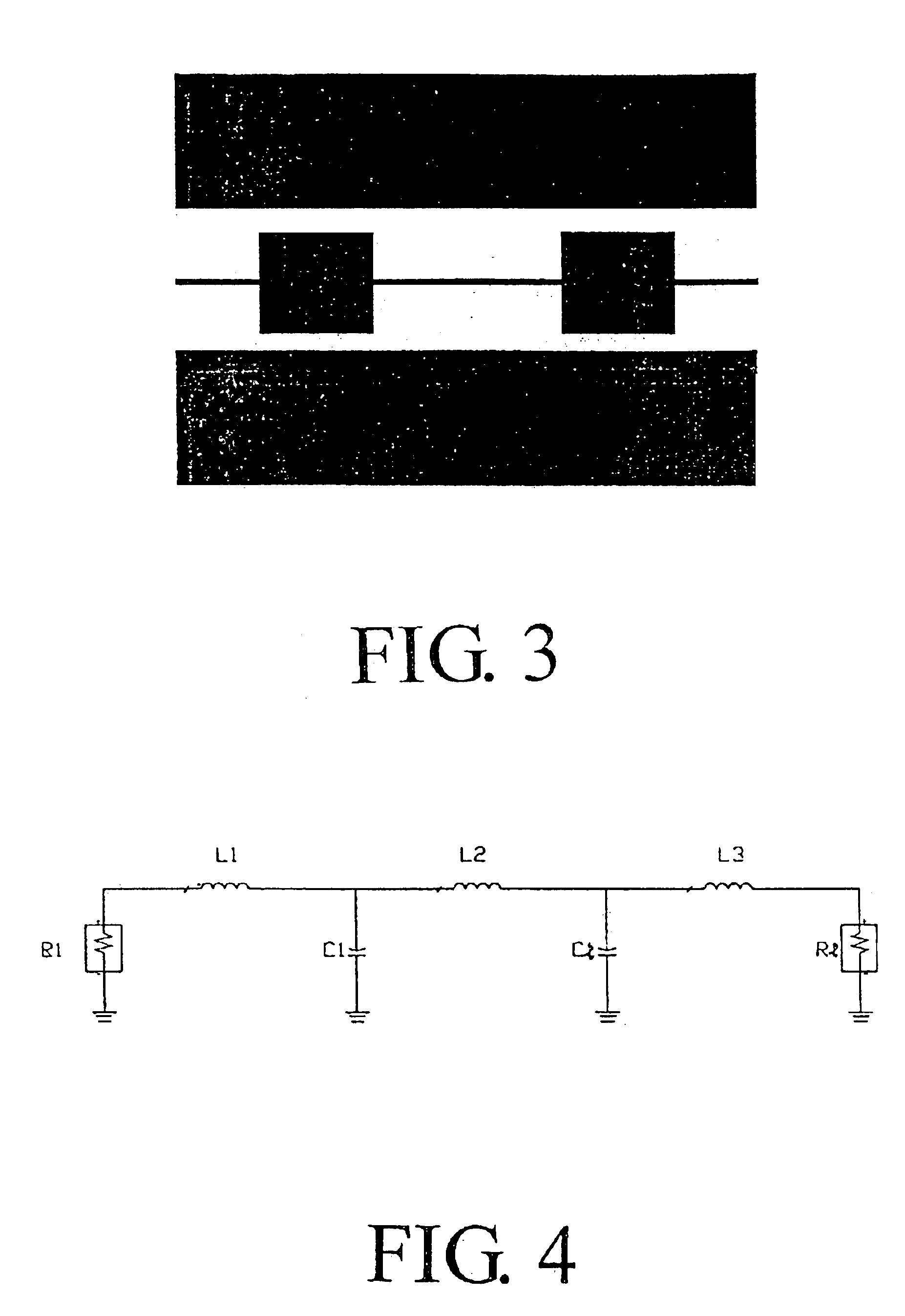
Referring to the equivalent circuit for a five order low pass filter according to the present invention shown in FIG. 4, and its structure shown in FIG. 5, the equivalent circuit includes three inductances L1, L2, and L3 connected in series, and two capacitance C1, C2 connected in parallel. The structure thereof shown in FIG. 5 includes a substrate 10 preferably made of Al2O3 with Σr=9.8, and a thickness of preferably 200˜350 μm; a first dielectric layer 11 enclosed over the substrate 10, the dielectric layer 11 is preferably made of Benzocyclobutene having a low dielectric constance (K≈2.6), a low tangential loss (tan θ≈0.002), and a preferable thickness of 2˜3 μm, in addition to the property of low dielectric constant and low tangential loss, it should be of good adhesiveness with the metallic materi...


PUM


Abstract

The present invention discloses a miniaturized multi-layer coplanar wave guide low pass filter including: a substrate; a first dielectric layer formed on and enclosing said substrate; a first metallic pattern layer formed on said first dielectric layer; a second dielectric layer formed on said first metallic pattern layer; wherein several via holes being formed on said second dielectric layer; a second metallic pattern layer formed on said second dielectric layer, wherein said via holes formed on said second dielectric layer are filled up with the metal thereof; a third dielectric layer formed on said second metallic pattern layer, wherein several via holes being formed on said third dielectric layer; and a third metallic pattern layer formed on said third dielectric layer, wherein said via holes formed on said third dielectric layer are filled with the metal thereof.

Description

BACKGROUND OF THE INVENTION1. Field of the InventionThe present invention relates to a miniaturized multi-layer coplanar wave guide low pass filter, and more particularly, to a miniaturized multi-layer coplanar wave guide low pass filter which is capable of enlarging the region of the characteristic impedance of a transmission line and miniaturizing the size of a filter by utilizing a multi-layer coplanar wave guide.2. Description of the Prior ArtAs it is well known, a filter is essentially composed of series inductors and parallel capacitors.A low pass filter plays an important role on the microwave circuit, and is used to eliminate noises in a frequency change over circuit. However, the operation frequency in a new generation mobile communication system has been raised up to 30 GHz and above so as to cope with the trend of rapid development of the modern radio communication technology, and the design of transmission and distribution mode should be considered to operate the electro...

Claims


Application Information

Patent Timeline
IPC IPC(8): H01P11/00H01P1/201H01P1/20
CPCH01P1/2013H01P11/007H01P11/003
Inventor SHIN-HSUAN, TSENGCHENG-KUO, LINYIN-CHING, WANGFAN-HSIU, HUANGYI-JEN, CHAN
Owner CYNTEC
Why Eureka
Try Eureka