
Narrow lateral waveguide laser

a laser and narrow waveguide technology, applied in lasers, semiconductor devices, semiconductor lasers, etc., can solve the problems of large size and power levels that are not suitable for some applications, and the gain-guided laser diodes have strong instabilities, etc., to achieve the effect of low optical power density and easy growth

Inactive Publication Date: 2005-01-18
WISCONSIN ALUMNI RES FOUND
View PDF17 Cites 6 Cited by
  • Summary
  • Abstract
  • Description
  • Claims
  • Application Information

AI Technical Summary

Benefits of technology

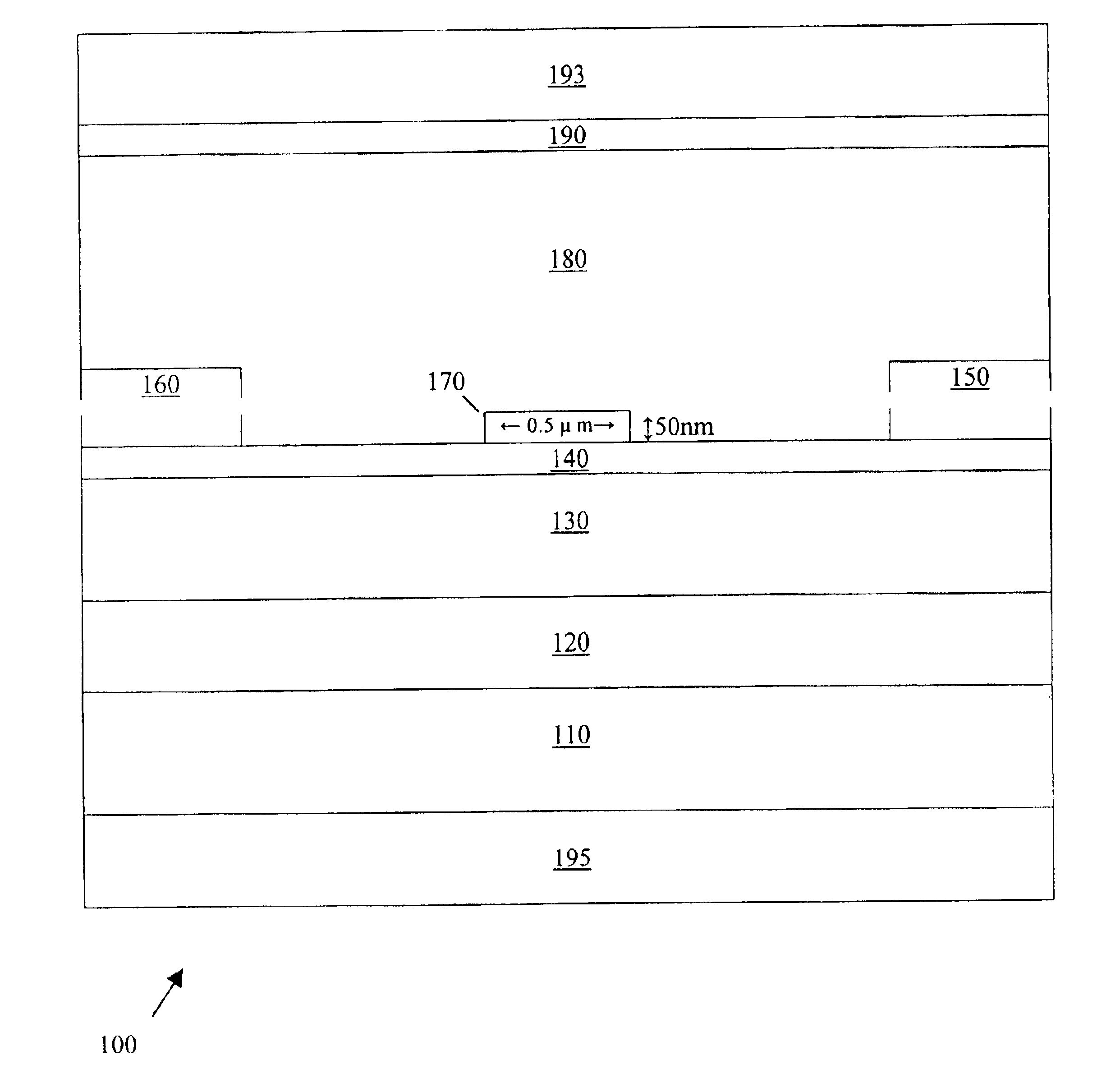
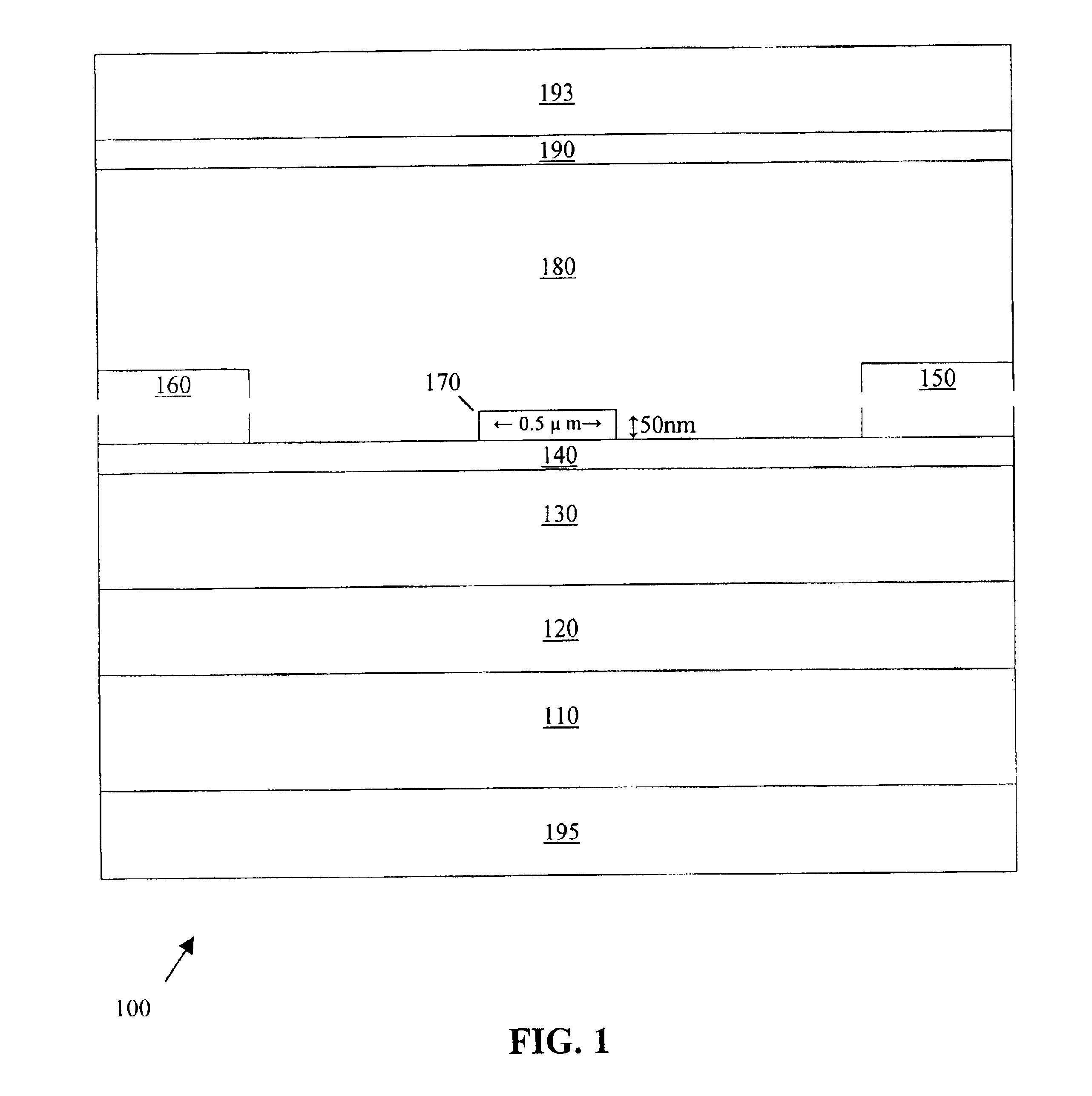
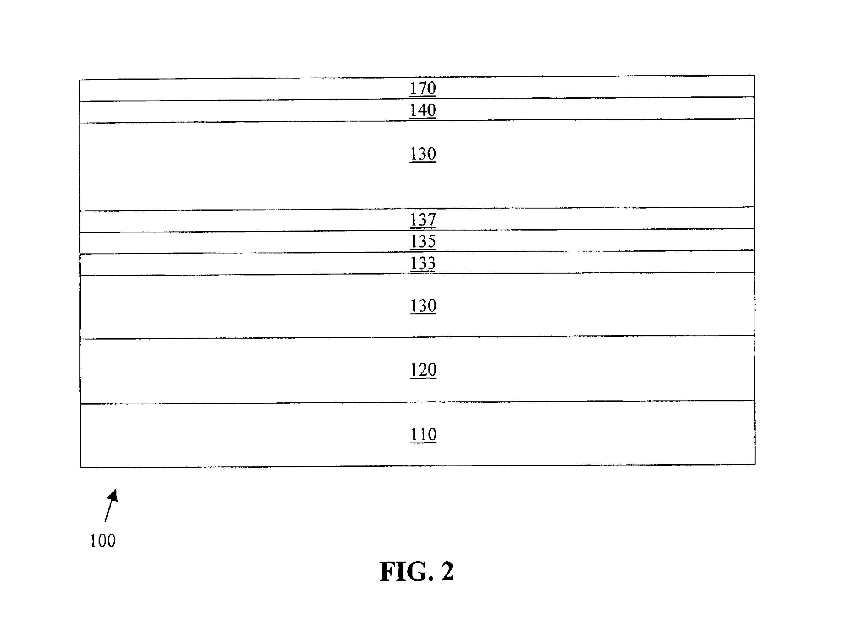
In accordance with the invention, a semiconductor laser can include at least one quantum well, one or more transverse waveguide layers, a first cladding layer located below the waveguide layers, a lateral guide structure located close to the active region, blocking structures located proximate the lateral guide structure and providing lateral confinement of current to a region surrounding the lateral guide structure, and a second cladding layer located above the lateral guide structure. The lateral guide structure has a first index and the second cladding layer has a second index. The first index is higher than the second index. In accordance with the invention, a narrow lateral waveguide can be used in conjunction with a suitable transverse structure to achieve a low optical power density and single lateral mode operation with a structure that may be easily grown via MOCVD and processed with standard semiconductor techniques. The operation of the narrow lateral waveguide is not dependent on a particular transverse structure, and may be combined with a transverse narrow waveguide, broad waveguide, or other structure which features a large transverse spot size.

Problems solved by technology

However, at high power levels, gain-guided laser diodes have strong instabilities and generate broad, highly-astigmatic multi-peaked beams.
Such sizes and power levels can be inadequate for some applications, such as pumping optical amplifiers for long range transmission.
A high optical power density at the output facet of a semiconductor laser negatively affects both the maximum attainable optical power from the laser before the onset of catastrophic optical mirror damage (COMD) and the long-term reliability of the device.
When devices of both types are operated at the same total output power the higher power density in the device with the narrow optical mode will contribute to greater local facet heating and therefore accelerated facet degradation relative to the device with the wider optical mode, leading to reduced device lifetimes and reliability.
If a laser can support undesirable modes above threshold in addition to the desired mode, coupling inefficiencies and kinked ex-fiber power-current relationships can occur.
However, the techniques required to construct a tapered structure are not easily incorporated into a standard MOCVD regrowth manufacturing process.

Method used


Image

  • Narrow lateral waveguide laser
  • Narrow lateral waveguide laser
  • Narrow lateral waveguide laser

Examples


Embodiment Construction

In the following description, for purposes of explanation, numerous specific details are set forth to provide a thorough understanding of exemplary embodiments of the invention. It will be evident, however, to one skilled in the art that the invention may be practiced without these specific details. In other instances, structures and devices are shown in diagram form to facilitate description of the exemplary embodiments.

Exemplary embodiments of an edge-emitting semiconductor laser incorporating a narrow waveguide design and a method of making the same are disclosed herein. The narrow waveguide expands the lateral mode size, creating a large modal spot size and ensuring higher-order modes are beyond cutoff. Separate current confinement allows the current injection region to match the mode size. The resulting device exhibits single-mode operation with a large spot-size to high output powers.

The laser of the present invention is well suited for coupling to single mode optical fibers, ...


PUM


Abstract

As edge-emitting semiconductor laser incorporating a narrow waveguide design is disclosed. The narrow waveguide expands the lateral mode size, creates a large modal spot size, and insures higher-order modes are beyond cutoff. Separate current confinement allows the current injection region to match the mode size. The resulting device exhibits single-mode operation with a large spot-size to high output powers.

Description

FIELD OF THE INVENTIONThe present invention relates generally to semiconductor laser diodes, including techniques for laterally confining the optical output of semiconductor laser diodes. More particularly, the present invention relates to narrow lateral waveguide lasers and methods of making the same.BACKGROUND OF THE INVENTIONIn general, a semiconductor laser is a diode device in which a forward bias voltage is applied across an active layer, which is surrounded by one or more waveguide layers, which in turn are surrounded by a pair of cladding layers. One cladding layer is an n-doped layer and the other is a p-doped layer so that excess electrons from the n-doped layer and excess holes from the p-doped layer are injected through the wavelength layers and into the active layer by the bias voltage, where they recombine. At current levels above a threshold value, stimulated emission occurs and a monochromatic, highly-directional beam of light is emitted from the active layer. A reso...

Claims


Application Information

Patent Timeline
Patent Type & Authority Patents(United States)
IPC IPC(8): H01S5/00H01SH01S5/22H01S5/223
CPCH01S5/2231H01S5/0655H01S2301/18H01S5/2218
Inventor MAWST, LUKE J.TANSU, NELSONNESNIDAL, MICHAEL P.MEASSICK, STEVENSTIERS, ERIC W.HANSEN, DARREN M.GOODNOUGH, TROY J.
Owner WISCONSIN ALUMNI RES FOUND
Learn More