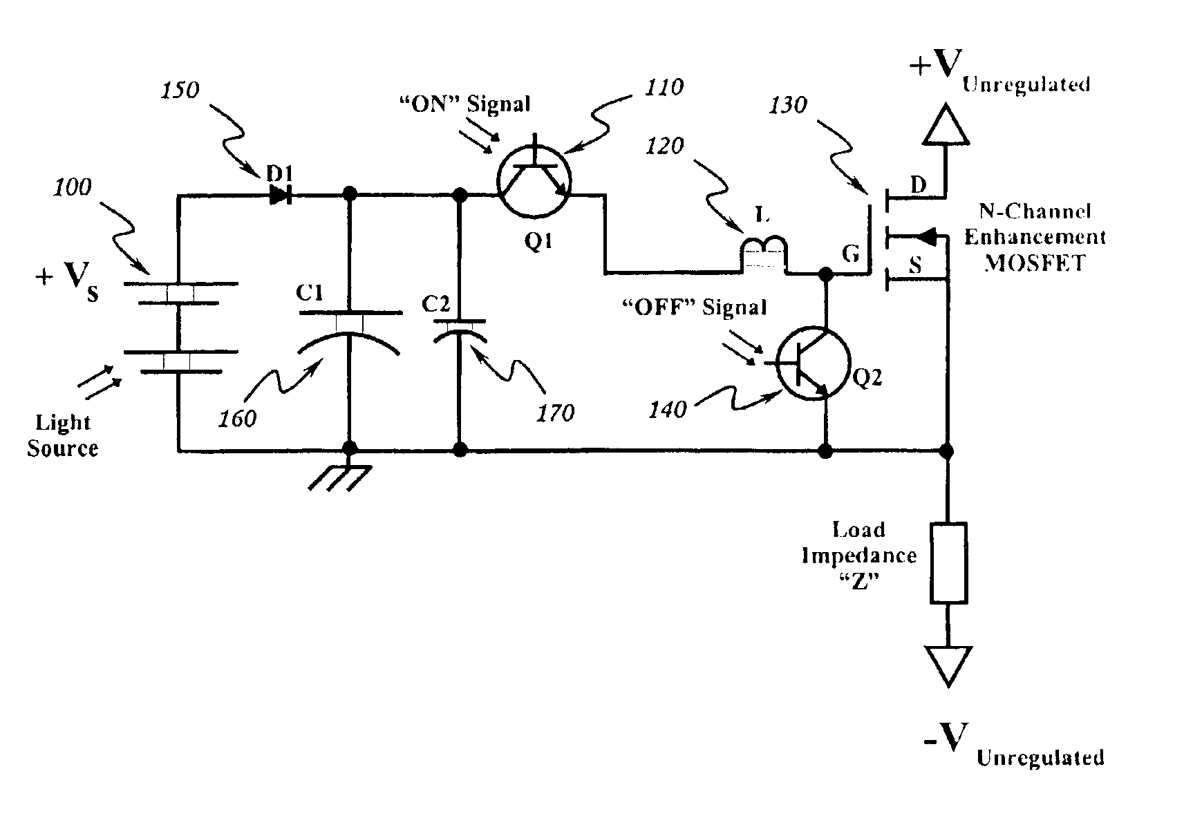
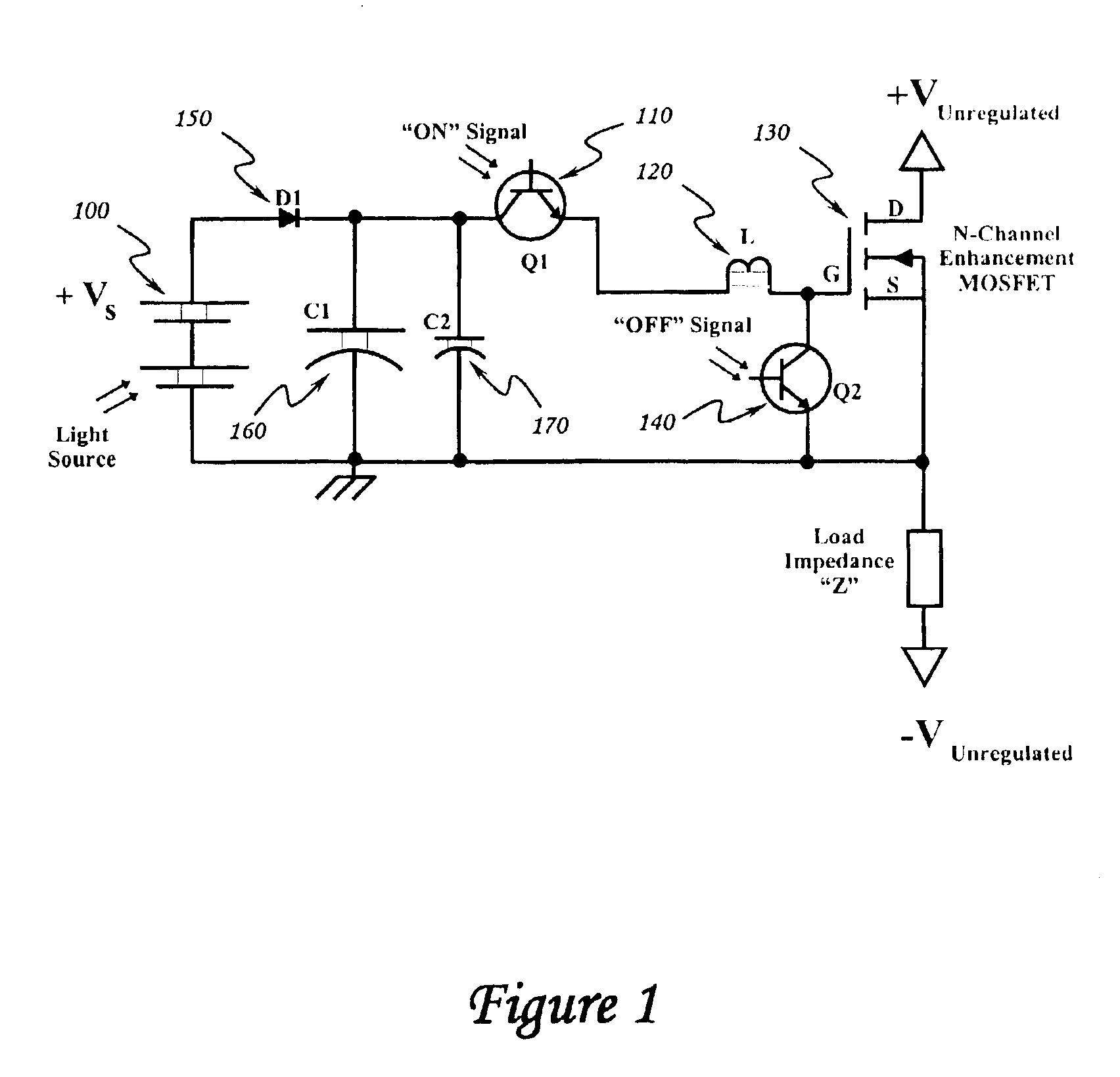
Optically isolated bias control circuit
a bias control circuit and optically isolated technology, applied in the field of optically isolated bias control circuits, can solve the problems of low frequency of useful operation, large and heavy transformers capable of low frequency operation, and high cost of high-voltage transformers designed to isolate high-voltage voltages
- Summary
- Abstract
- Description
- Claims
- Application Information
AI Technical Summary
Benefits of technology
Problems solved by technology
Method used
Image
Examples
embodiment # 1
Alternate Embodiment #1
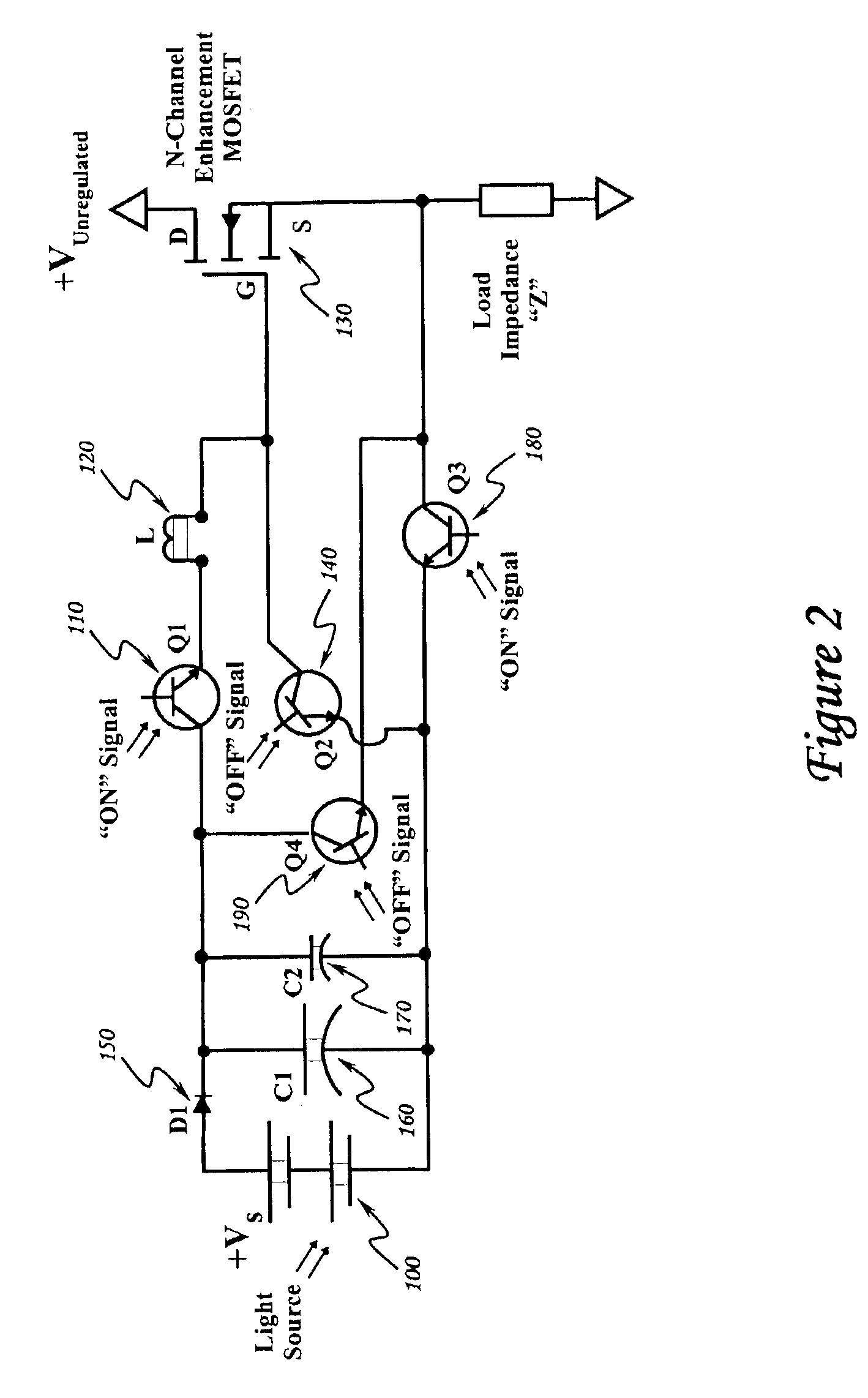
Referring to FIG. 2, a first alternative embodiment of the invention is depicted. The first alternate embodiment of the present invention involves the use of two additional optically isolating photo-transistors Q3180 and Q4190. This embodiment effectively reverses the polarity of the bias voltage source 100 applied to the gate-to-source circuit of the MOSFET 130 in order to force the circuit off as fast as it is forced on. This circuit has enhanced noise immunity due to a negative gate-to-source voltage and may be able to operate with pulses of faster rise and fall times than the embodiment depicted in FIG. 1 with a given gate control voltage, but it requires two additional optically isolating devices.
Referring to FIG. 4, a series connection of either embodiment of the gate bias control circuits (see FIG. 1 or FIG. 2) is depicted that enables operating voltages greater than a single MOSFET can hold off. The series of gate bias control circuits must receive the...
PUM
 Abstract
Description
Claims
Application Information
 - R&D
- Intellectual Property
- Life Sciences
- Materials
- Tech Scout
- Unparalleled Data Quality
- Higher Quality Content
- 60% Fewer Hallucinations
Browse by: Latest US Patents, China's latest patents, Technical Efficacy Thesaurus, Application Domain, Technology Topic, Popular Technical Reports.
© 2025 PatSnap. All rights reserved.Legal|Privacy policy|Modern Slavery Act Transparency Statement|Sitemap|About US| Contact US: help@patsnap.com


