
Two-step process for nickel deposition

a nickel deposition and nickel technology, applied in the direction of semiconductor devices, basic electric elements, electrical equipment, etc., can solve the problems of increasing difficulty in maintaining performance and reliability, shortening the transistor, etc., and achieve the effect of reducing the shorting of the transistor

Inactive Publication Date: 2005-01-11
ADVANCED MICRO DEVICES INC
View PDF1 Cites 12 Cited by
  • Summary
  • Abstract
  • Description
  • Claims
  • Application Information

AI Technical Summary

Benefits of technology

An object of the present invention is a method of manufacturing a semiconductor device to overcome the aforementioned disadvantage and reduce transistor shorting due to the formation of a thin nickel silicide layer on the spacers.
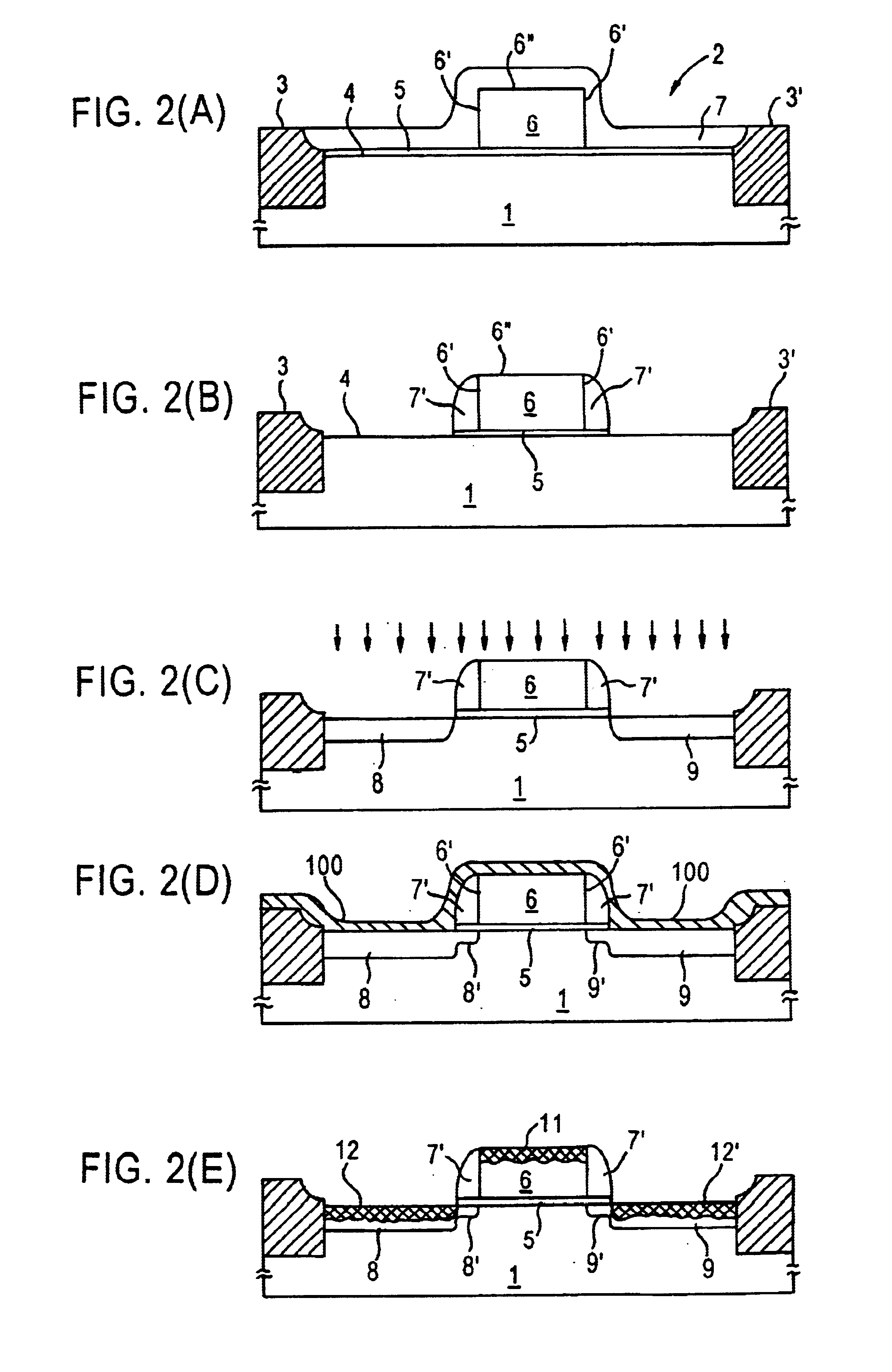
It is still a further object of the invention to form a blanket layer of nickel is formed by the sequential steps of: forming a first layer of nickel by sputtering in a oxygen gas atmosphere; and the forming a second layer of nickel on the first layer by sputtering in an argon gas atmosphere, whereby undesirable nickel silicide formation on the sidewall spacers during subsequent processing is substantially eliminated.

Problems solved by technology

As device scaling plunges into the deep sub-micron ranges, it becomes increasingly difficult to maintain performance and reliability.
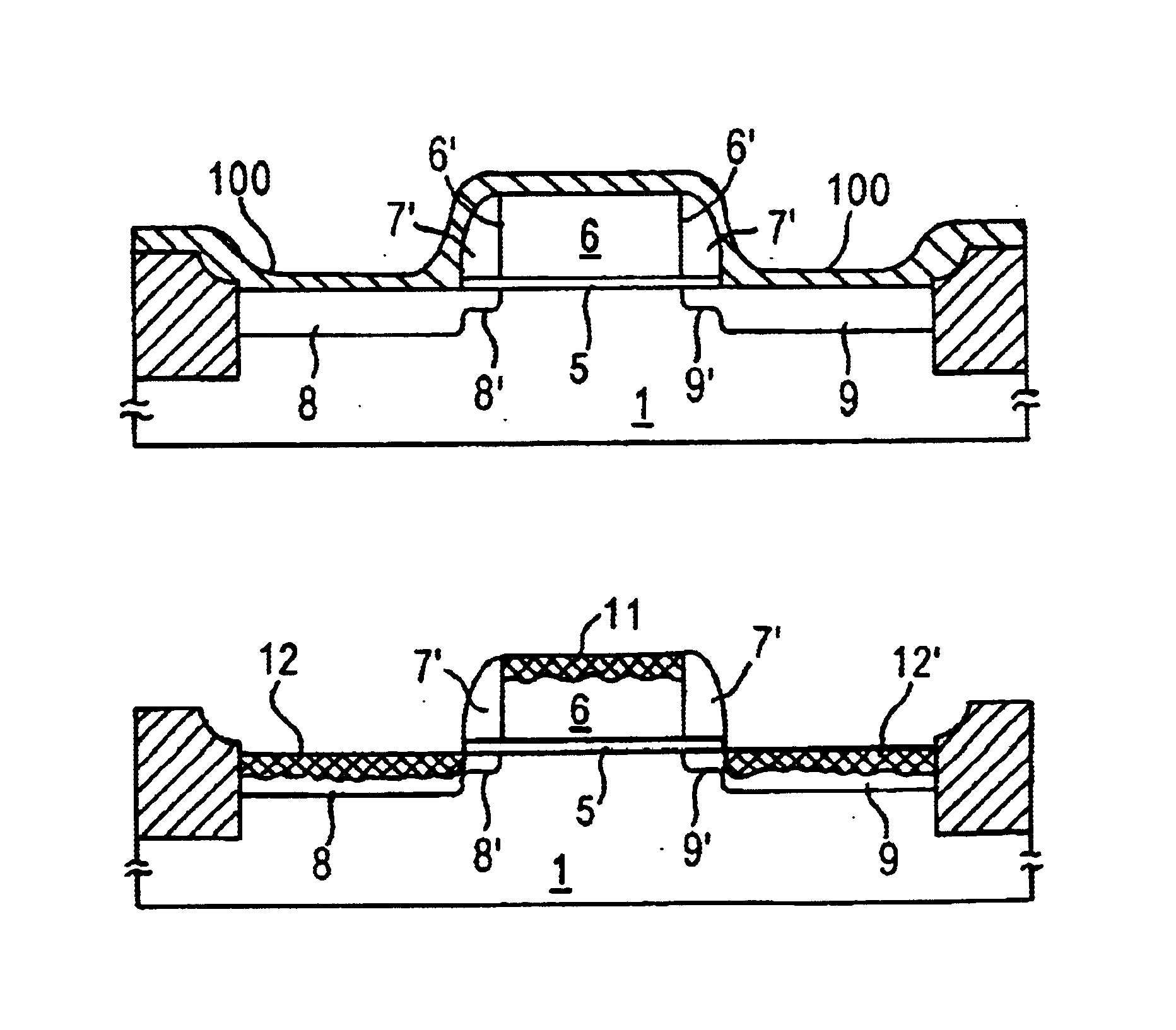
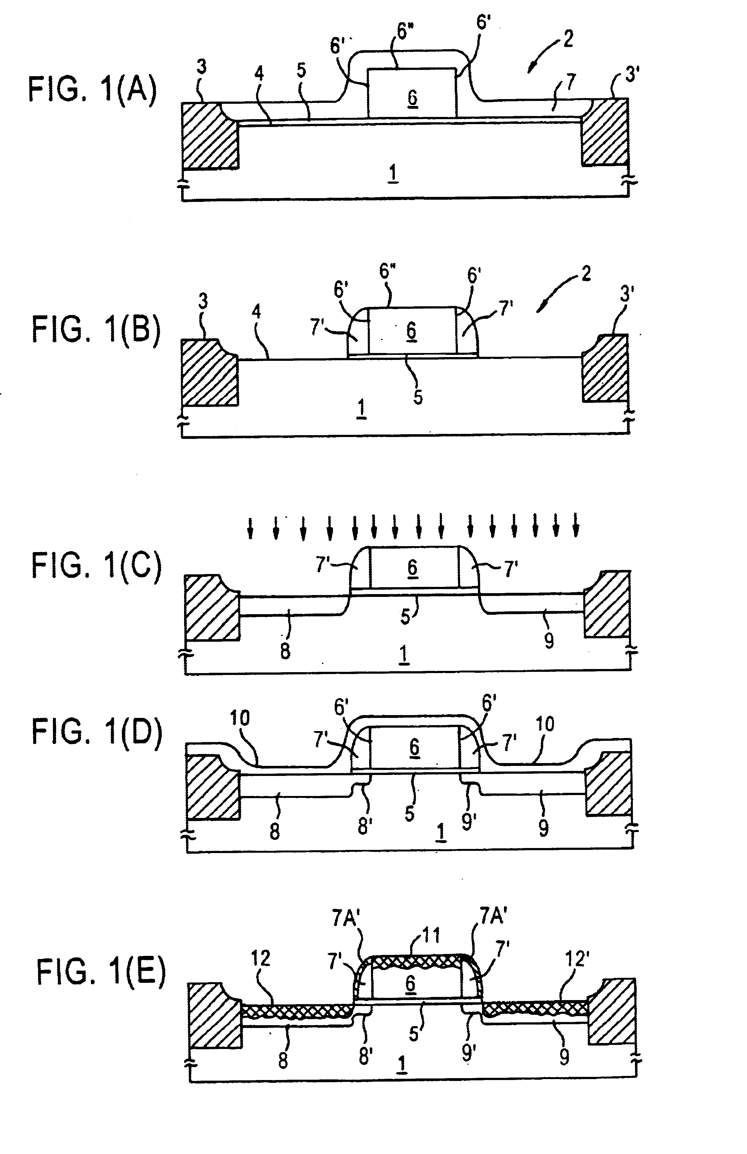
Formation of the thin film of nickel silicide 7A′ on the outer surface of sidewall spacers 7′ disadvantageously results in the fonlation of a conductive bridge to the source, thereby shorting out the transistor.

Method used


Image

  • Two-step process for nickel deposition
  • Two-step process for nickel deposition
  • Two-step process for nickel deposition

Examples


Embodiment Construction

The present invention addresses and solves a problem arising from manufacturing submicron-dimensioned, ultra-shallow junction MOS and CMOS transistors suitable for use in high-density integration semiconductor devices. More specifically, the present invention addresses and solves a problem stemming from the formation of a thin nickel silicide layer on the side wall spacers using conventional methods of manufacture, thus disadvantageously causing shorting out of the transistor because of the formation of a conductive path between the gate and the source. Moreover, the inventive methodology provides increased device reliability while increasing product yield.

The invention is illustrated in FIGS. 2(A)-2(E). The figures show the sequence of processing steps for manufacturing a MOS transistor embodiment of the present invention. However, the methodology illustrated in FIGS. 2(A)-2(E) is not limited to MOS devices. As will be apparent, the inventive process may be readily adapted for use ...


PUM

PropertyMeasurementUnit
widthaaaaaaaaaa
thicknessaaaaaaaaaa
electrically conductiveaaaaaaaaaa

Abstract

Sub-micron dimensioned, ultra-shallow junction MOS and / or CMOS transistor devices are formed by a salicide process wherein a blanket nickel layer is formed in contact with the exposed portions of the substrate surface adjacent the sidewall spacers, the top surface of the gate electrode, and the sidewall spacers. Embodiments include forming the blanket layer of nickel is formed by the sequential steps of: (i) forming a layer of nickel by sputtering with oxygen gas; and, (ii) forming a layer of nickel by sputtering with argon gas. The two step process for forming the blanket layer of nickel advantageously prevents the formation of nickel silicide on the outer surfaces of the insulative sidewall spacers.

Description

FIELD OF THE INVENTIONThe present invention relates to a method of manufacturing a semiconductor device comprising nickel silicide contacts to source / drain regions. The present invention has particular applicability in manufacturing reliable high density semiconductor devices with submicron design features, shallow junction depths and nickel silicide contacts to source / drain regions.BACKGROUND ARTCurrent demands for high density and performance associated with ultra large scale integration require design rules of about 0.18 microns and under, increased transistor and circuit speeds and improved reliability. As device scaling plunges into the deep sub-micron ranges, it becomes increasingly difficult to maintain performance and reliability.Salicide processing involves deposition of a refractory metal that forms a compound with silicon, but does not react with silicon oxides, nitrides, or oxynitrides under normal processing conditions. Refractory metals commonly employed in the salicid...

Claims


Application Information

Patent Timeline
Patent Type & Authority Patents(United States)
IPC IPC(8): H01L21/02H01L21/336H01L21/285
CPCH01L29/665H01L21/28518
Inventor BERTRAND, JACQUES J.KLUTH, GEORGE J.
Owner ADVANCED MICRO DEVICES INC
Learn More