
Solderless electronics packaging

a technology of electronics packaging and solderless technology, applied in the direction of fixed connections, connection contact material, instruments, etc., can solve the problems of loop inductance production within ic packages and electronic assemblies that cannot provide solderless or socketable packages, and the amount of loop inductance produced within ic packages can increase to unacceptable levels

Inactive Publication Date: 2005-01-11
INTEL CORP
View PDF42 Cites 66 Cited by
  • Summary
  • Abstract
  • Description
  • Claims
  • Application Information

AI Technical Summary

Problems solved by technology

However, it does not provide a solderless or socketable package.
As the internal circuitry of ICs, such as processors, operates at higher and higher clock frequencies, and as ICs operate at higher and higher power levels, the amount of loop inductance produced within IC packages and electronic assemblies can increase to unacceptable levels.

Method used


Image

  • Solderless electronics packaging
  • Solderless electronics packaging
  • Solderless electronics packaging

Examples


Embodiment Construction

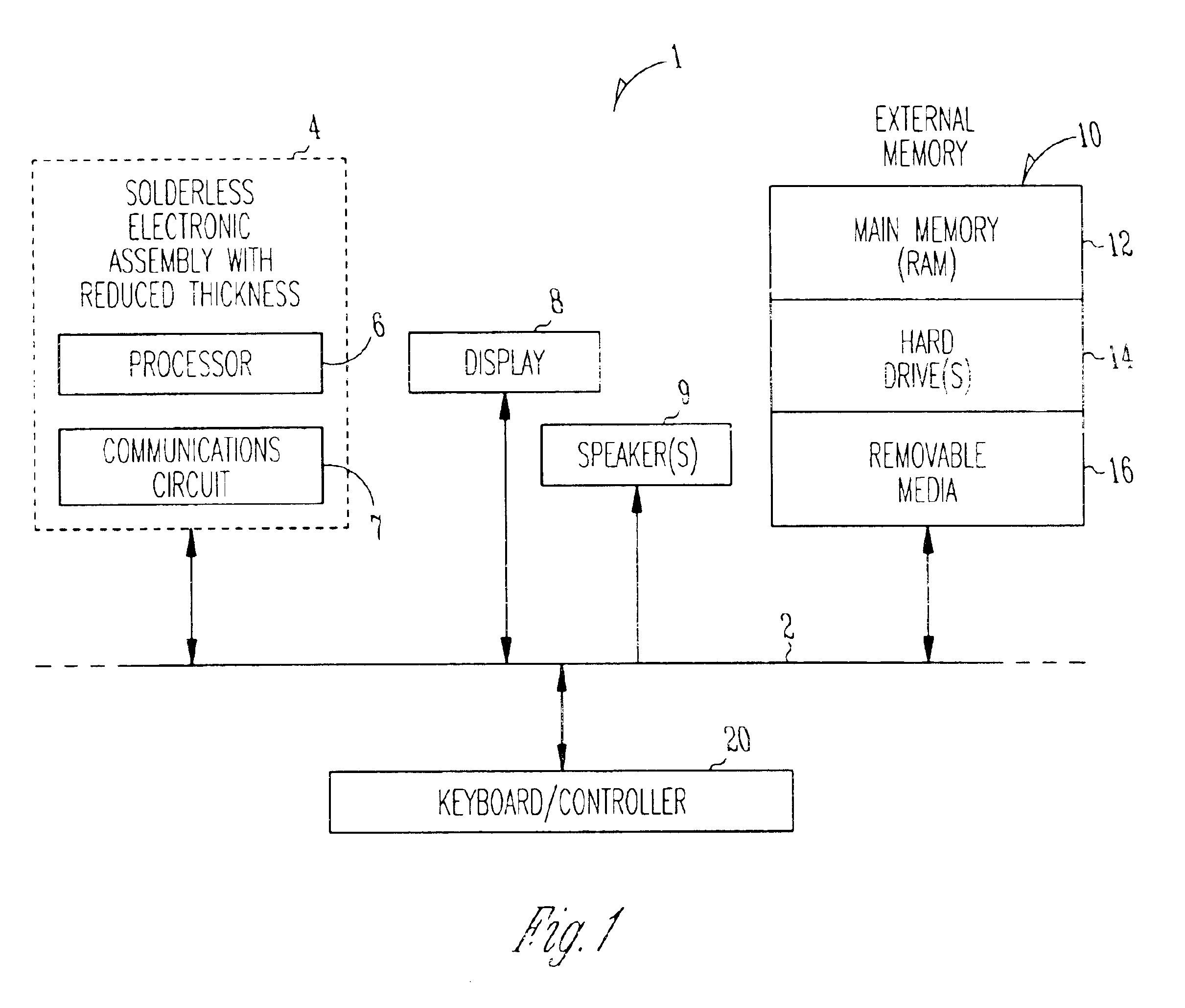
In the following detailed description of embodiments of the inventive subject matter, reference is made to the accompanying drawings which form apart hereof, and in which are shown by way of illustration specific preferred embodiments in which the inventive subject matter may be practiced. These embodiments are described in sufficient detail to enable those skilled in the art to practice the inventive subject matter, and it is to be understood that other embodiments may be utilized and that mechanical, chemical, electrical, and procedural changes may be made without departing from the spirit and scope of the inventive subject matter. Such embodiments of the inventive subject matter may be referred to, individually and / or collectively, herein by the term “invention” merely for convenience and without intending to voluntarily limit the scope of this application to any single invention or inventive concept if more than one is in fact disclosed. The following detailed description is, th...


PUM

PropertyMeasurementUnit
Electrical conductivityaaaaaaaaaa
aaaaaaaaaa

Abstract

To decrease the thickness, or stack height, of an electronics package, the package includes a solderless compression connector between an integrated circuit (IC) package and a substrate such as a printed circuit board (PCB). In one embodiment, the IC package is mounted on the substrate using a land grid array arrangement. Corresponding lands on the IC package and substrate are coupled using a solderless compression connector. The compression connector includes a plurality of electrically conductive elements, such as compressible button contacts, and an apertured support that aligns the button contacts with corresponding lands on the IC package and substrate. In another embodiment, the connector includes electrically conductive pins embedded in a thin plastic sheet. In a further embodiment, the connector includes a microcrystalline film having electrically conductive crystals. In a further embodiment, the compression connector is used within an IC package to couple an IC to an IC package substrate. Methods of fabrication, as well as application of the package to an electronic assembly, an electronic system, and a data processing system, are also described.

Description

TECHNICAL FIELDThe inventive subject matter relates generally to electronics packaging. More particularly, the inventive subject matter relates to an electronic package that includes an integrated circuit package or an integrated circuit coupled to a substrate with a solderless compression connector, and to manufacturing methods related thereto.BACKGROUND INFORMATIONIntegrated circuits (ICs) are typically assembled into electronic packages by physically and electrically coupling them to a substrate made of organic or ceramic material. One or more IC packages can be physically and electrically coupled to a substrate such as a printed circuit board (PCB) or motherboard to form an “electronic assembly”. The “electronic assembly” can be part of an “electronic system”. An “electronic system” is broadly defined herein as any product comprising an “electronic assembly”. Examples of electronic systems include computers (e.g., desktop, laptop, hand-held, server, etc.), wireless communication...

Claims


Application Information

Patent Timeline
IPC IPC(8): H01L23/02H01L23/055H01L23/10H01L23/48H01L23/433H01L23/498H01L23/34H05K7/10H05K3/32H05K13/04
CPCH01L23/055H01L23/4334H01L23/49827H01L23/49833H01L23/49866H05K3/325H05K7/1061H05K13/046H01L23/10Y10T29/49169H01L2224/73204H01L2224/73253H01L2924/01004H01L2924/01025H01L2924/01046H01L2924/01078H01L2924/01079H01L2924/1433H01L2924/15311H01L2924/16152H01R12/57Y10T29/49126H01L2224/16225Y10T29/49155Y10T29/49147Y10T29/4913Y10T29/49117H01L2224/81101H01L2224/05573H01L2224/05568H01L2924/00014H01L2224/32245H01L2924/16195H01L2224/05599
Inventor SATHE, AJIT V.WERMER, PAUL H.
Owner INTEL CORP
Learn More