
Fabrication of high resistivity structures using focused ion beams

Inactive Publication Date: 2005-01-04
FEI COMPANY
View PDF18 Cites 45 Cited by
  • Summary
  • Abstract
  • Description
  • Claims
  • Application Information

AI Technical Summary

Benefits of technology

An object of the invention is to provide microscopic conductive structures having high electrical resistance.

Problems solved by technology

Current ion beam deposition methods that deposit tungsten or other metal-based materials by the decomposition of precursor gases are incapable of depositing conductors having high electrical resistance.
There is no method for producing structures having resistances in the range of one megohm to one hundred megohms.

Method used


Image

  • Fabrication of high resistivity structures using focused ion beams
  • Fabrication of high resistivity structures using focused ion beams
  • Fabrication of high resistivity structures using focused ion beams

Examples


Embodiment Construction

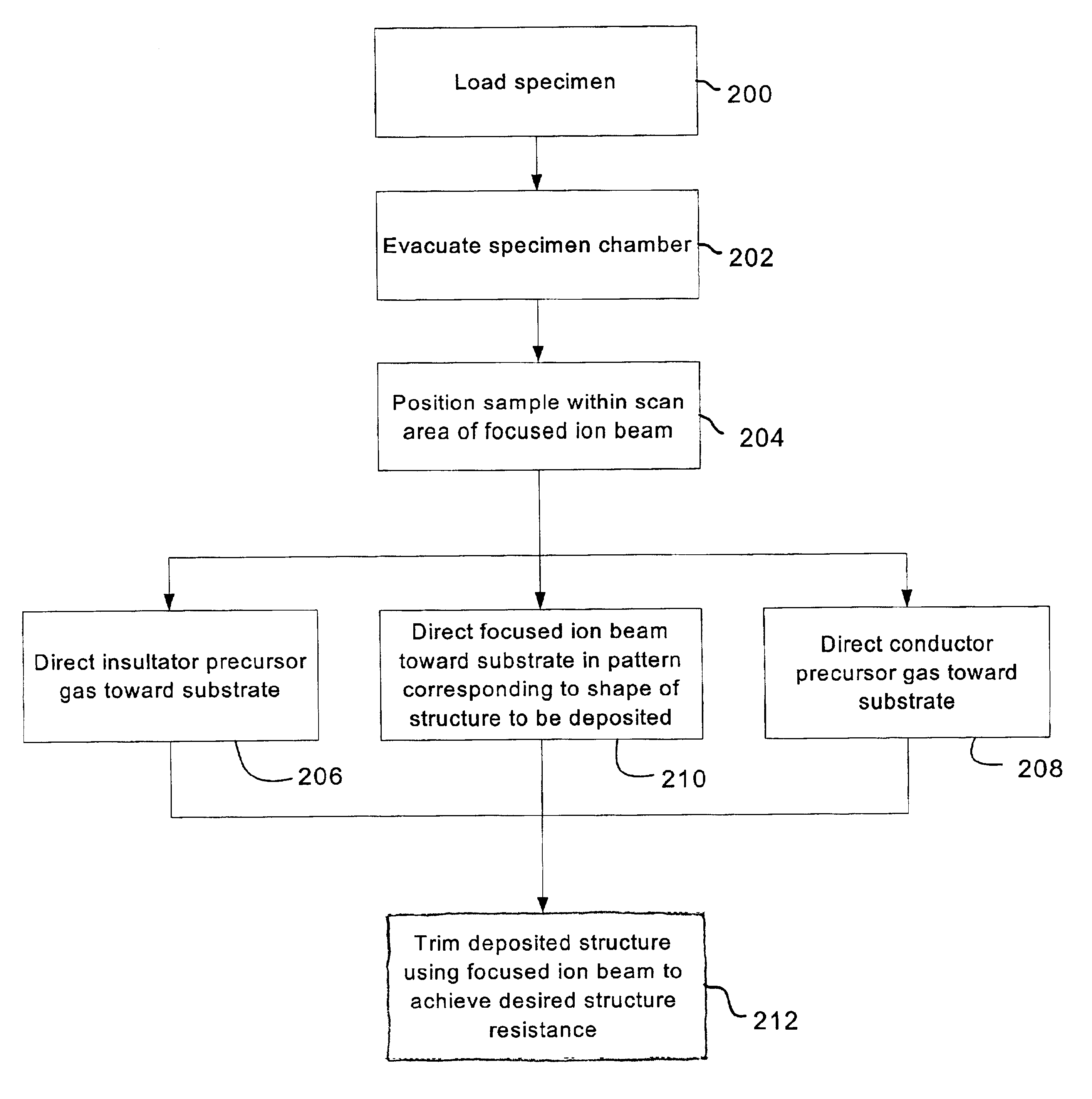
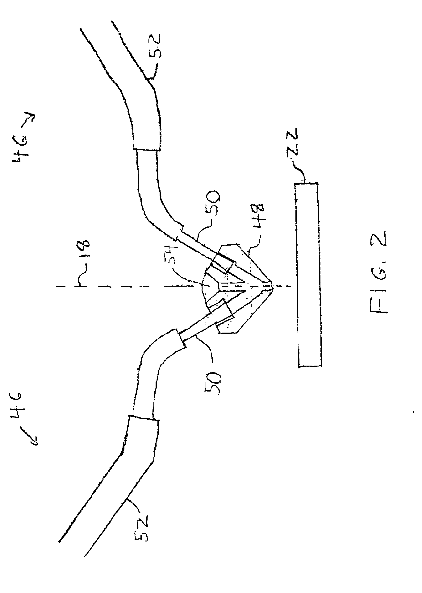
FIG. 1 shows schematically a typical focused ion beam system 8 used to implement a preferred embodiment of the present invention. Focused ion beam system 8 includes an evacuated envelope 10 having an upper neck portion 12 within which are located a liquid metal ion source 14 and a focusing column 16 including extractor electrodes and an electrostatic optical system. Ion beam 18 passes from source 14 through column 16 and between electrostatic deflection mechanism schematically indicated at 20 toward specimen 22, which comprises, for example, a semiconductor device positioned on movable X-Y stage 24 within lower chamber 26. Lower chamber 26 can be vacuum isolated from evacuated envelope 10 by a valve 62.

An ultra high vacuum pump, such as an ion pump 28, is employed for evacuating neck portion 12. The chamber 26 is evacuated with turbo-molecular and mechanical pumping system 30 under the control of vacuum controller 32. The vacuum system provides within chamber 26 a vacuum of between ...


PUM

PropertyMeasurementUnit
Lengthaaaaaaaaaa
Electric potential / voltageaaaaaaaaaa
Sheet resistanceaaaaaaaaaa

Abstract

The present invention provides a method for creating microscopic high resistivity structures on a target by directing a focused ion beam toward an impact point on the target and directing a precursor gas toward the impact point, the ion beam causing the precursor gas to decompose and thereby deposit a structure exhibiting high resistivity onto the target. The precursor gas preferably contains a first compound that would form a conductive layer and a second compound that would form an insulating layer if each of the first and second compounds were applied alone in the presence of the ion beam.

Description

TECHNICAL FIELD OF THE INVENTIONThe invention relates to the use of charged particle beam systems to fabricate conductive microscopic structures having high electrical resistivity and, in particular, to the use of focused ion beam systems to fabricate electronic circuit elements.BACKGROUND OF THE INVENTIONFocused ion beams (FIBs) can be focused to a spot smaller than one tenth of a micron. Because of their small spot size, focused ion beam systems are used to create and alter microscopic structures. Focused ion beams can micro-machine material by sputtering or etching, that is, physically knocking atoms or molecules from the target surface. Focused ion beams can also be used to deposit material, using a precursor gas that adheres to the specimen surface and decomposes in the presence of the ion beam to leave a deposit on the surface. FIB systems are widely used in the semiconductor industry to alter prototype integrated circuits by depositing metallic paths to create new connections...

Claims


Application Information

Patent Timeline
IPC IPC(8): C23C16/04H01L21/285H01L21/02C23C16/48
CPCC23C16/047H01J37/08H01L28/24H01L21/28562H01J2237/31749H01J2237/31737
Inventor BASSOM, NEIL J.MAI, TUNG
Owner FEI COMPANY
Learn More