
Programmable memory built-in self-test combining microcode and finite state machine self-test

a programming memory and self-testing technology, applied in the field of memory structure testing, can solve the problems of memory cells, relatively delicate devices, and low process cost of fabrication, and achieve the effects of low process cost, small memory cell area, and low cost of fabrication

Inactive Publication Date: 2003-11-18
GOOGLE LLC
View PDF15 Cites 34 Cited by
  • Summary
  • Abstract
  • Description
  • Claims
  • Application Information

AI Technical Summary

Problems solved by technology

Design of storage devices and processes for their fabrication have become quite sophisticated and have resulted in very low process cost for fabrication and very small memory cell area.
Nevertheless, memory cells, particularly of the dynamic type which store data capacitively, are relatively delicate devices and may be subject to damage of deterioration after being placed in service.
However, access to embedded memories for testing is often difficult, particularly where chip space and external connections are at a premium.
The amount of chip space which can be efficiently allocated to a BIST is very limited, generally to about 2% of the area of the storage devices to be tested.
Because of the feedback of a memory component in complex dependent memory structures, testing is complicated and generally results in high test logic overhead, particularly for the large number of combinations of operations with which such a memory must be exercised.
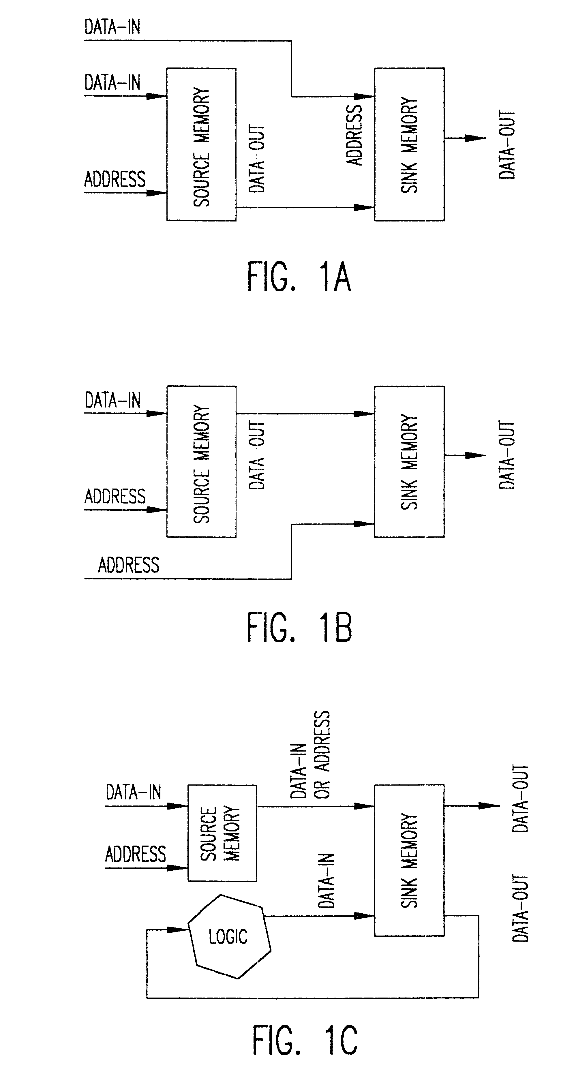
Accessing these buses is only possible through the embedded memory structure and requires test patterns with sequential behavior since they are a part of the feedback loop in the complex dependent memory structure.
Testing of complex embedded multi-port memory structures requires an especially complex test algorithm which, in turn, requires a large number of instructions and a large microcode-based controller which, in general, cannot be provided within the 2% area overhead constraint alluded to above.
Therefore, programmable BIST architectures are not efficiently applied to complex multi-port memory structures.
The only alternative to the area overhead would be to reduce thoroughness of the test procedure which is not feasible due to the high reliability of the memory structure which must be assured.
Further, it should be appreciated that the design effort and cost of developing and compiling large instruction sets for programmable BIST architectures capable of testing multi-port complex memory structures and the design of BIST circuits incorporating them on a chip greatly increases chip design costs.
Further, the provision of instructions in programmable ROM is, itself, somewhat self-defeating since the testing of such programmable ROM is also difficult if the storage space is relatively large.

Method used


Image

  • Programmable memory built-in self-test combining microcode and finite state machine self-test
  • Programmable memory built-in self-test combining microcode and finite state machine self-test
  • Programmable memory built-in self-test combining microcode and finite state machine self-test

Examples


Embodiment Construction

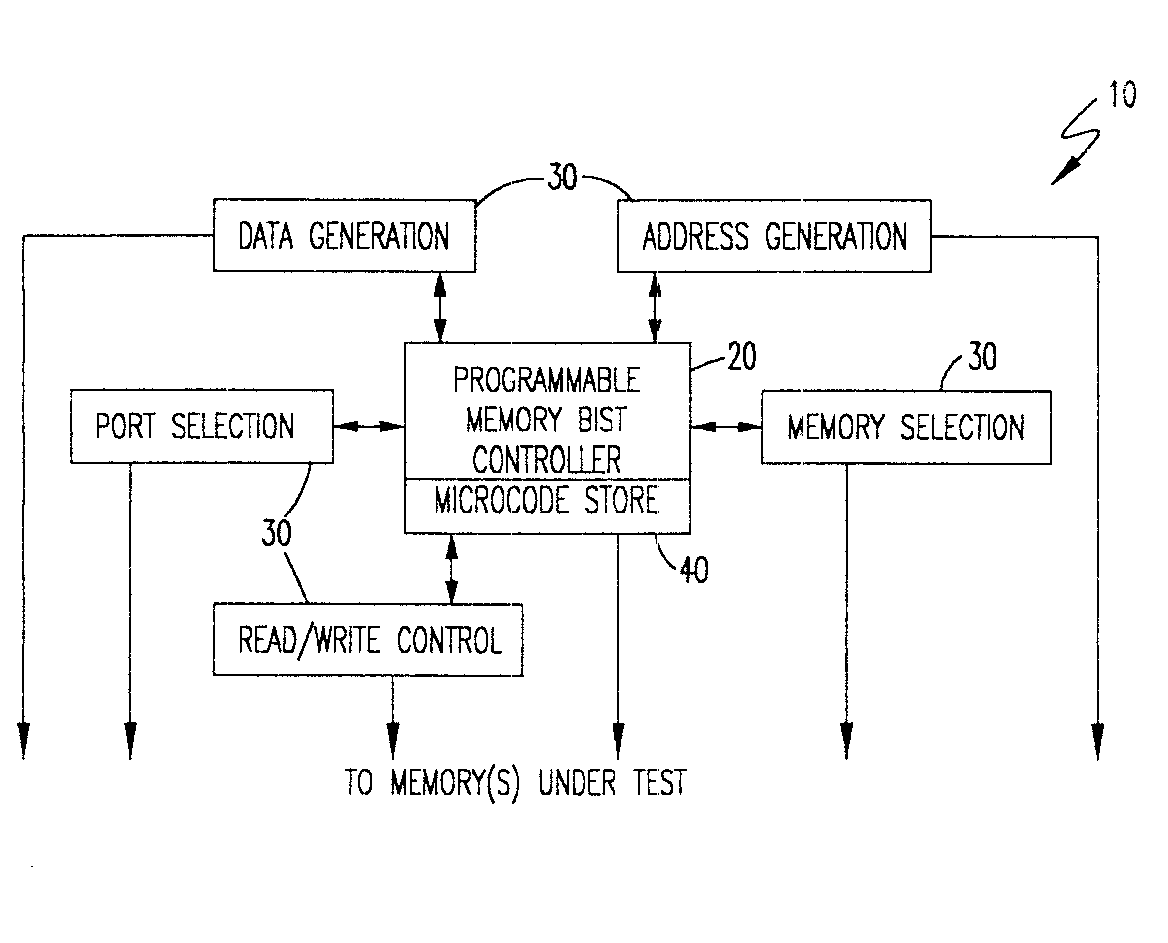
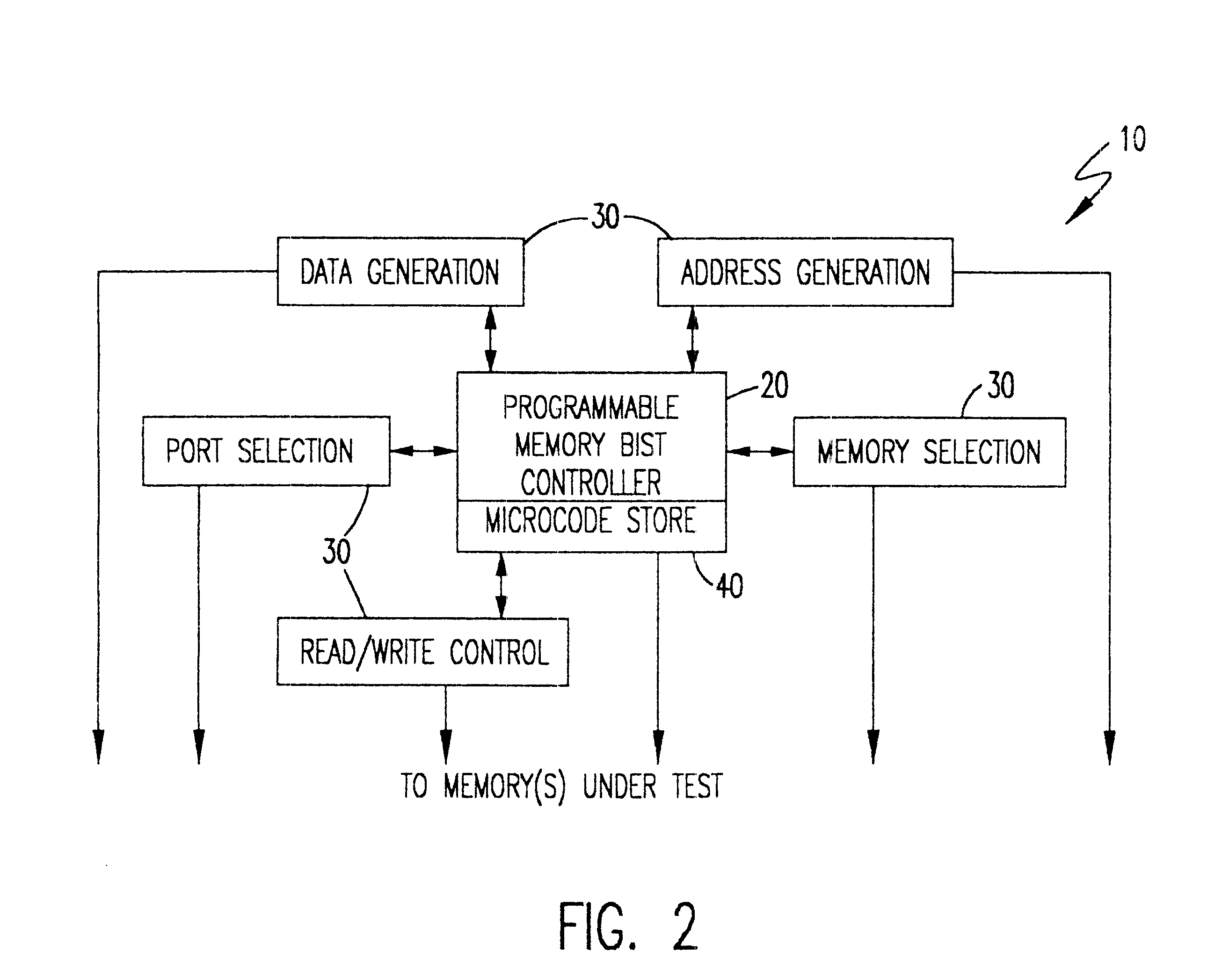
Referring now to the drawings, and more particularly to FIG. 4, there is shown a highly conceptualized diagram of the enhanced programmable memory BIST module in accordance with the invention. Some of the elements illustrated such as the instruction decoder 30 and microcode store 40 are substantially similar to the corresponding elements depicted in the programmable BIST architecture illustrated in FIG. 2 and discussed above. However, the microcode stored in microcode store 40 is altered somewhat from that used in the architecture of FIG. 2 as will be discussed below in connection with FIG. 5. The BIST controller 20 in accordance with the invention will be more fully discussed below in connection with FIG. 6.

A particularly distinctive feature of the BIST module 100 is the use of instruction generate modules 110 which comprise finite state machines (FSM). Conceptually, a finite state machine comprises a circuit which can assume any one of a finite number of states wherein changes bet...


PUM


Abstract

A finite state machine (FSM) is used to generate, in real time, potentially long sequences of signals which control generation of signals for application to a memory structure during a self-test procedure which is provided in hardware on the same chip with the memory structure. The FSM-based instruction generator requires much less area than is required for storage of a corresponding number of microcode instructions and allows the built-in self-test (BIST) controller to have a modular architecture permitting re-use of hardware designs for the BIST arrangement with consequent reduction of elimination of design costs of the BIST arrangement to accommodate new memory designs. The sequential nature of the operation of a finite state machine as it progresses through a desired sequence of states is particularly well-suited to controlling capture of signals where access to high. speed data transfer circuits cannot otherwise be accommodated.

Description

1. Field of the InventionThe present invention generally relates to the testing of memory structures and, more particularly, to testing of memory structures included in very large scale integrated circuits (VLSI).2. Description of the Prior ArtIncreases in integration density of integrated circuits has greatly increased the performance and functionality of the circuits which can be included on a single semiconductor chip. Increased functionality, of course requires increased circuit complexity and, at the present state of the art, many functionally differentiated regions such as adders, processors, logic arrays, buffers, decoders level converters and the like may be included on a single chip. These functionally differentiated regions are often designed to operate at different clock rates and even different voltages while being required to communicate with each other in a generally synchronized fashion.Design of storage devices and processes for their fabrication have become quite so...

Claims


Application Information

Patent Timeline
IPC IPC(8): G01R31/28G01R31/3187G11C29/04G11C29/16G01R31/3183G06F11/22G06F11/24G06F12/16G06F15/78G11C29/02G11C29/12
CPCG01R31/2891G11C29/16G01R31/3187G06F11/24
Inventor ADAMS, R. DEANECKENRODE, THOMAS J.GREGOR, STEVEN L.ZARRINEH, KAMRAN
Owner GOOGLE LLC
Learn More