
Method of catalyzing copper deposition in a damascene structure by plasma treating the barrier layer and then applying a catalyst such as iodine or iodine compounds to the barrier layer

a damascene structure and copper metal technology, applied in the direction of plasma technique, semiconductor/solid-state device details, coatings, etc., can solve the problems of limited copper filling properties, increased aspect ratio, and reduced contact siz

Inactive Publication Date: 2003-11-11
HYUNDAI ELECTRONICS IND CO LTD
View PDF12 Cites 9 Cited by
  • Summary
  • Abstract
  • Description
  • Claims
  • Application Information

AI Technical Summary

Benefits of technology

This approach improves the adhesion and filling properties of copper metal wiring by maximizing the absorption sites of the chemical enhancer, enhancing the step coverage and contact filling capabilities, thus addressing the limitations of existing methods.

Problems solved by technology

This current methodology, however, has a problem when applied to next-generation high-performance semiconductor devices since aluminum is higher in resistance than copper.
In the latter method, copper is limited in its filling property due to an abrupt reduction in the contact size and an increase in the aspect ratio.
Thus, applying the copper wiring to the next-generation semiconductor device or using aluminum wiring and electroplating causes many problems.
However, due to a lower deposition speed, this method has a limit in bulk filling.
Further, if the chemical enhancer is directly deposited on the diffusion barrier layer without deposition of a seed, the absorption property of the chemical enhancer is degraded.
Therefore, there is a problem that a filling property of a copper metal wiring will be degraded.

Method used


Image

  • Method of catalyzing copper deposition in a damascene structure by plasma treating the barrier layer and then applying a catalyst such as iodine or iodine compounds to the barrier layer
  • Method of catalyzing copper deposition in a damascene structure by plasma treating the barrier layer and then applying a catalyst such as iodine or iodine compounds to the barrier layer
  • Method of catalyzing copper deposition in a damascene structure by plasma treating the barrier layer and then applying a catalyst such as iodine or iodine compounds to the barrier layer

Examples


Embodiment Construction

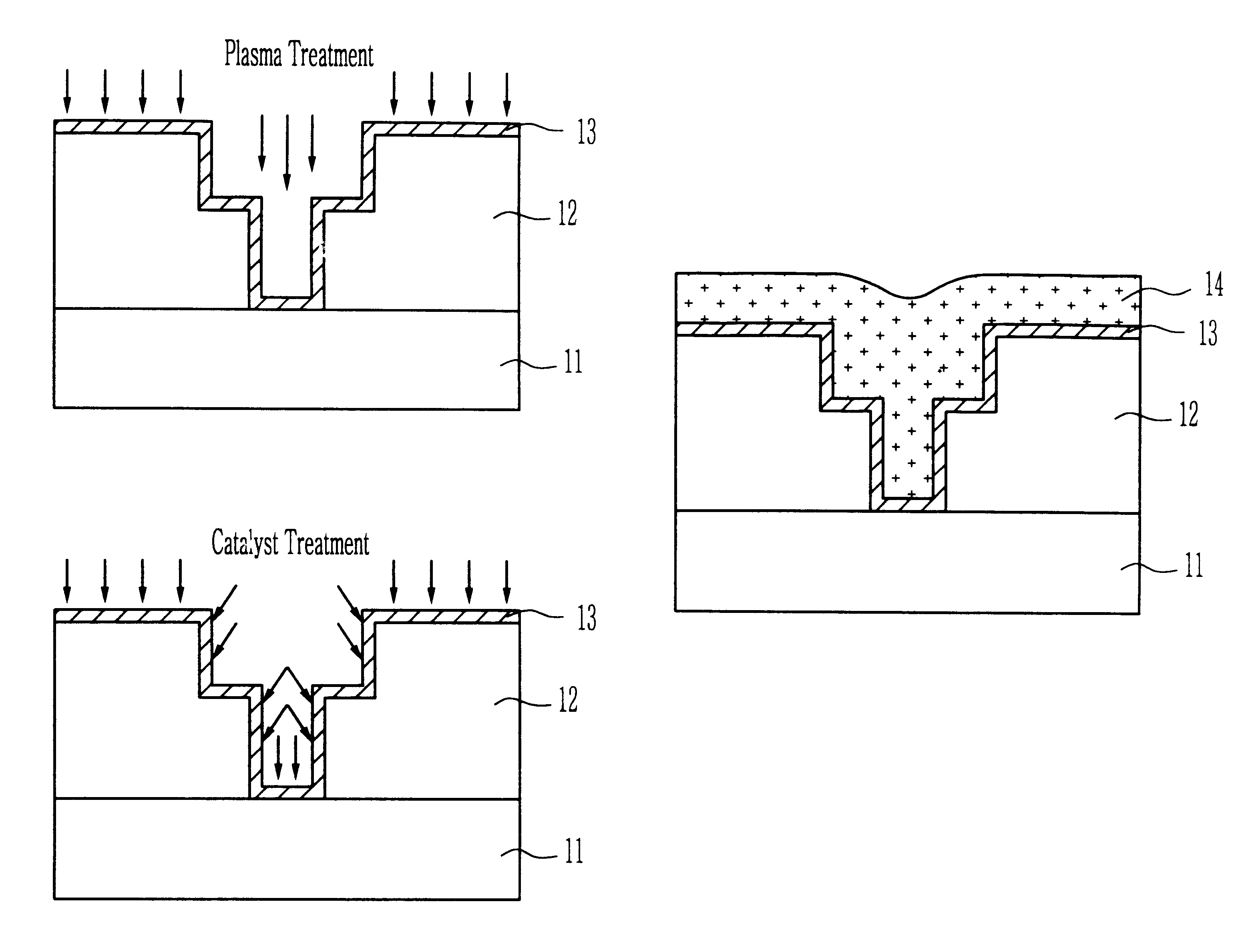
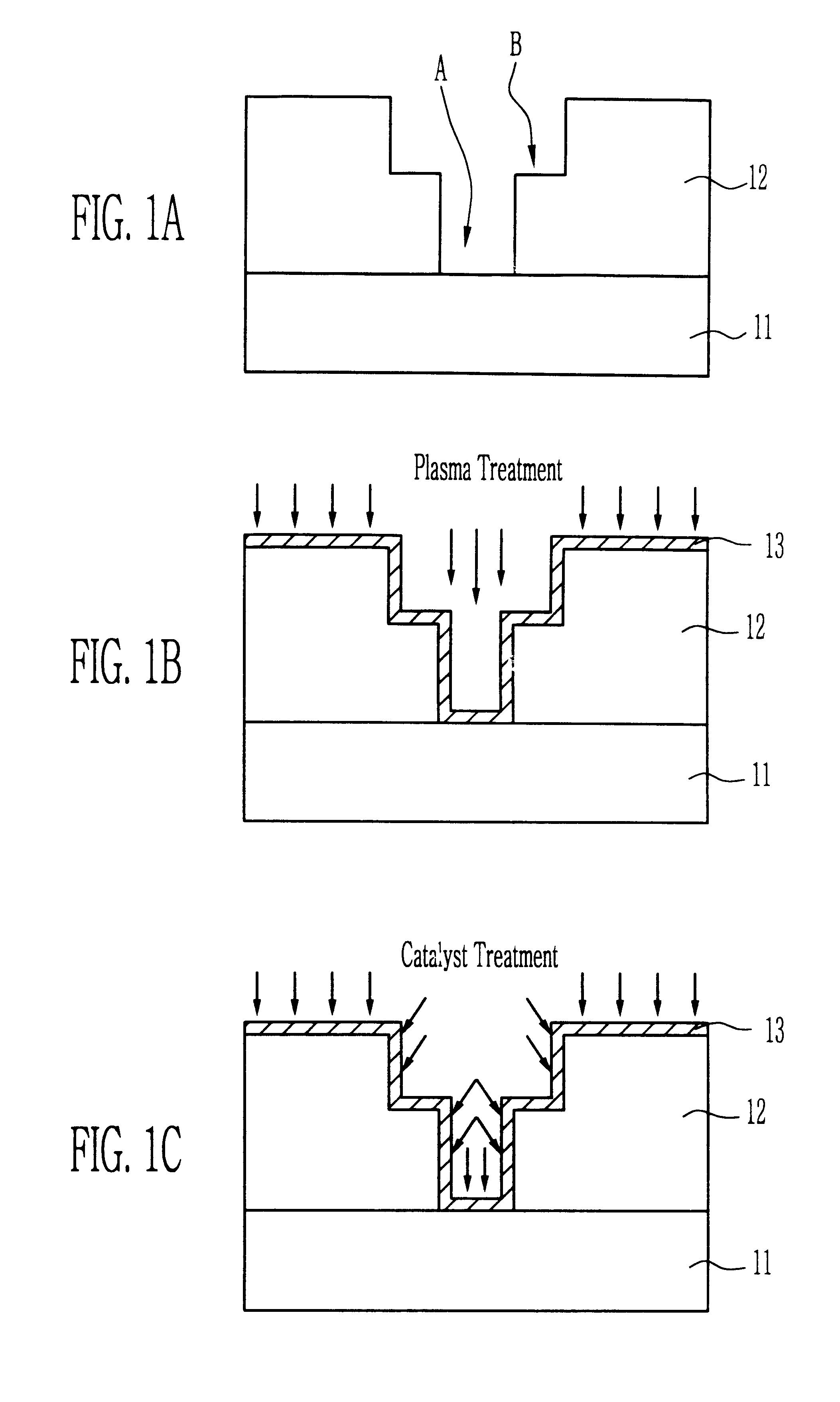
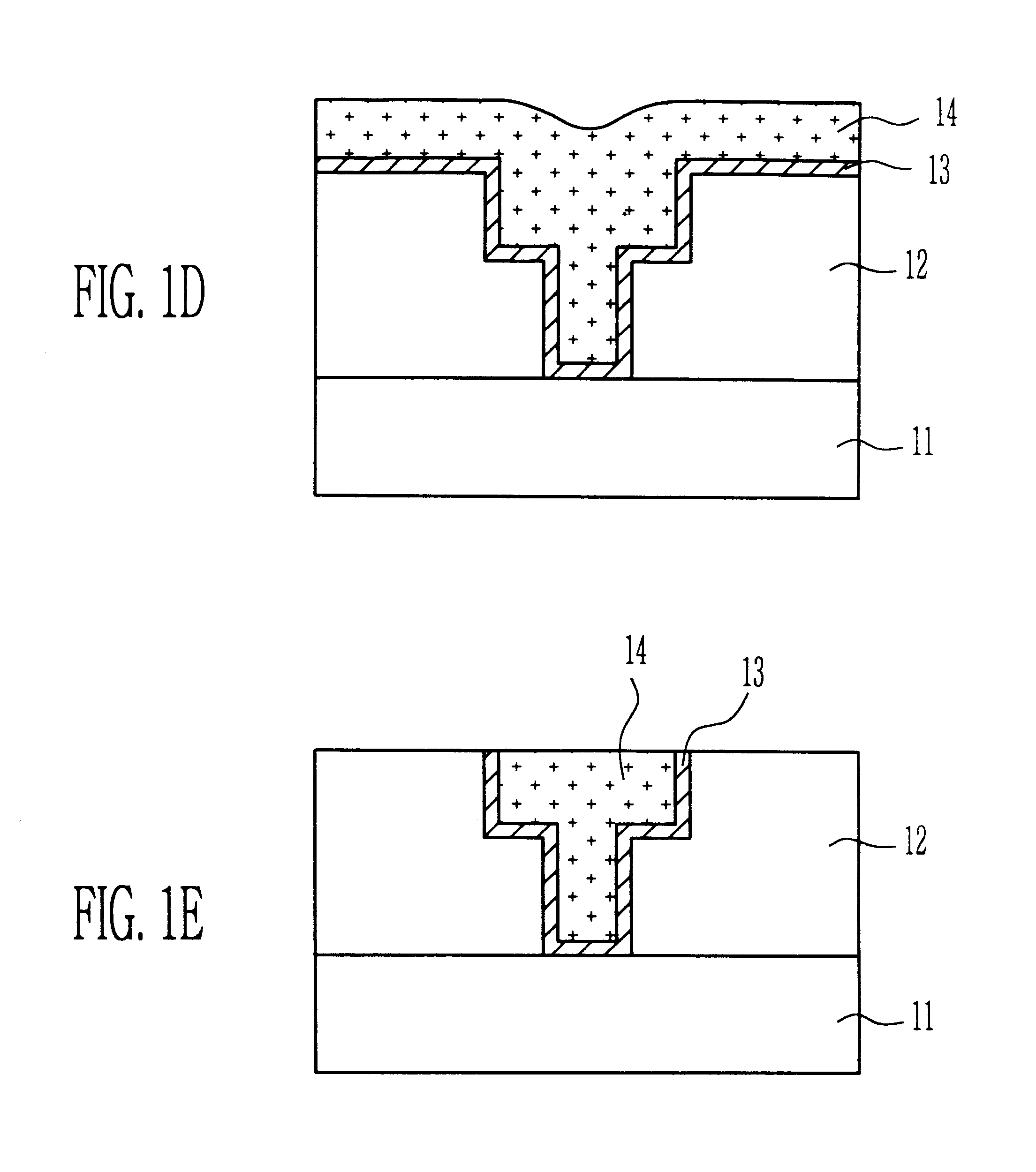
A method of manufacturing a copper metal wiring in a semiconductor device is disclosed that maximizes the adhesion property of a chemical enhancer on the surface of a diffusion barrier layer and thus improves the filling property of copper, by performing a plasma process after the chemical enhancer is deposited while a copper metal wiring is formed by means of a chemically enhanced chemical vapor deposition (CECVD) method. The invention will be described in detail by way of a preferred embodiment with reference to accompanying drawings.

As shown in FIG. 1A, an interlayer insulating film 12 is formed on a substrate 11 in which an underlying structure is formed. Then, the interlayer insulating film 12 is patterned by a single damascene or a dual damascene process to form a damascene pattern consisting of a contact A and a trench B. After that, a cleaning process is performed. At this time, the interlayer insulating film 12 is formed by depositing insulating materials having a low diele...


PUM

PropertyMeasurementUnit
temperatureaaaaaaaaaa
distanceaaaaaaaaaa

Abstract

A method of manufacturing a copper metal wiring in a semiconductor device, by which a plasma process is performed before a diffusion barrier layer is formed and a chemical pre-process using a chemical enhancer is performed so that copper is deposited to form a metal wiring by a chemically enhanced chemical vapor deposition (CECVD) method. The method allows the chemical enhancer to be adhered on the diffusion barrier layer uniformly and stably; therefore, improving the deposition property of a copper thin film.

Description

1. Field of the InventionThe invention relates generally to a method of manufacturing a copper metal wiring in a semiconductor device. More particularly, the invention relates to a method of manufacturing a copper metal wiring in a semiconductor device capable of increasing absorption sites of a chemical enhancer when copper is deposited to form a metal wiring through a chemically enhanced chemical vapor deposition (CECVD) method.2. Background of the InventionAs the performance of next-generation semiconductor device increases, the size of a contact is reduced and the aspect ratio increases. Therefore, when a metal wiring is formed, a good contact filling property and a step coverage is required.Presently, the manufacture of a metal wiring in a semiconductor device uses a method by which, after a titanium thin film (Ti) is deposited, aluminum (Al) is deposited thereon by a physical vapor deposition (PVD) method and a chemical vapor deposition (CVD) method, or tantalum (Ta) or tantal...

Claims


Application Information

Patent Timeline
Patent Type & Authority Patents(United States)
IPC IPC(8): H01L21/70H01L21/285H01L21/768H01L21/02C23C16/18C23C16/34H01L21/28H01L21/3205H01L23/52
CPCH01L21/28556H01L21/76838H01L21/76877H01L21/76862H01L21/76876H01L21/76843H01L21/28
Inventor PYO, SUNG GYUKIM, SI BUM
Owner HYUNDAI ELECTRONICS IND CO LTD
Learn More