Vertical layer type semiconductor device
a semiconductor and vertical layer technology, applied in the direction of semiconductor devices, electrical equipment, transistors, etc., can solve the problems of reducing the breakdown voltage (drain-source voltage), increasing the breakdown voltage, and not providing flexibility in the design criterion of the current capacity and the breakdown voltage of the semiconductor
- Summary
- Abstract
- Description
- Claims
- Application Information
AI Technical Summary
Problems solved by technology
Method used
Image
Examples
embodiment 2
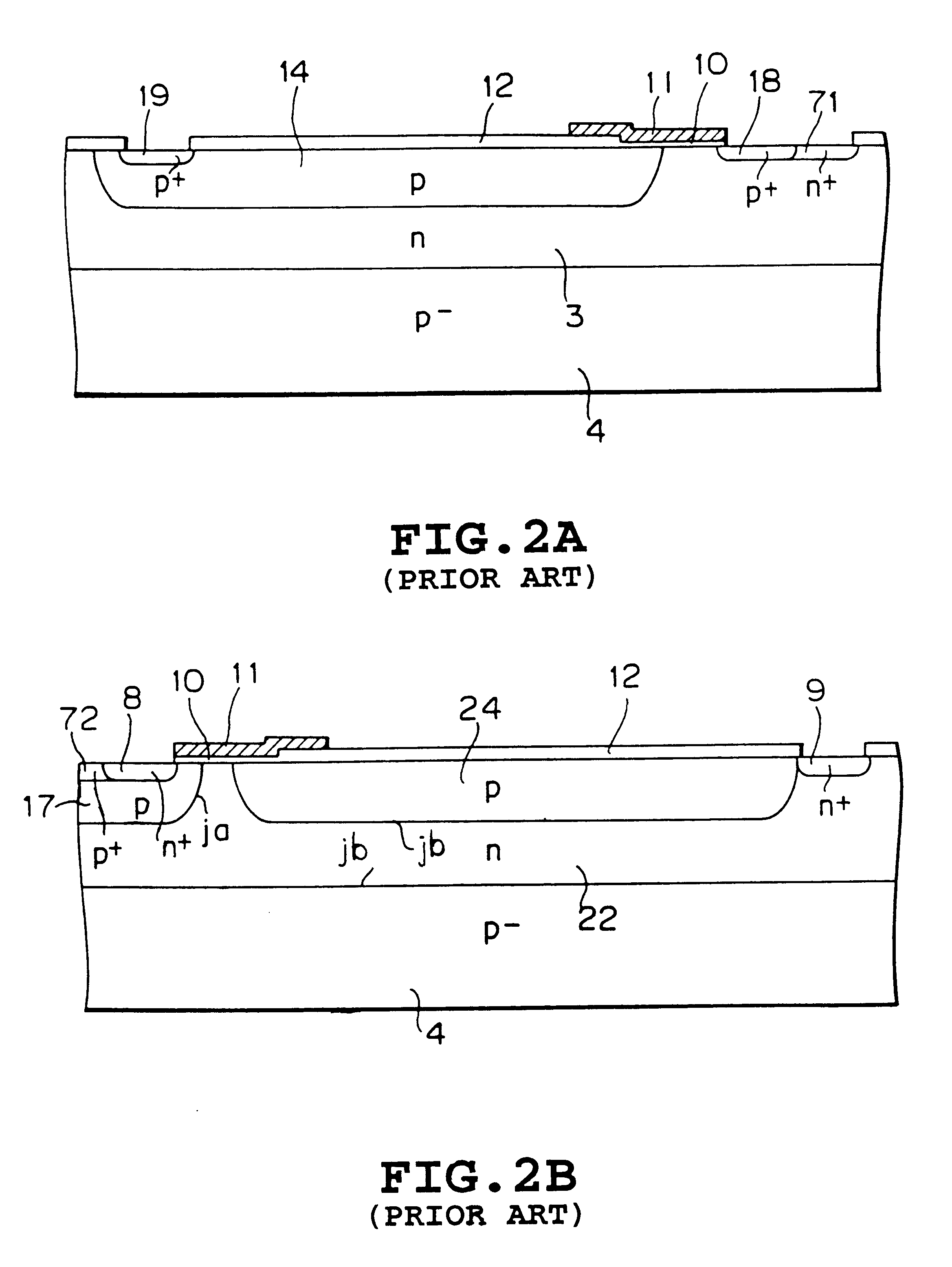
Referring now to FIGS. 7A to 7C, a double diffused type n-channel MOSFET (hereinafter, also referred as a double diffused MOSFET) will be described in detail as a second preferred embodiment of the present invention. In these Figures, FIG. 7A is a plan view showing the double diffused MOSFET, FIG. 7B is a cross sectional view along a line 7B--7B in FIG. 7A, and FIG. 7C is a cross sectional view along a line 7C--7C in FIG. 7A.
The double diffused MOSFET of the present embodiment has the same structure as the conventional double diffused MOSFET shown in FIGS. 2A and 2B except in the structure of drain / drift region. As shown in the figure, the double diffused MOSFET of the present embodiment comprises a drain / drift region 122 formed on a p.sup.- -type or n-type semiconductor layer 4, a gate electrode 11 with a filed plate formed on the drain / drift region 122 through a gate insulation film 10, a p-type channel diffusion region 17 in the shape of a well formed on a portion of the semicond...
embodiment 3
FIGS. 8A to 8C show a lateral SOI-MOSFET as a third preferred embodiment of the present invention. In these figures, FIG. 8A is a plan view of the lateral SOI-MOSFET, FIG. 8B is a cross sectional view along a line 8B--8B in FIG. 8A, and FIG. 8C is a cross sectional view along a line 8C--8C in FIG. 8A.
The lateral SOI-MOSFET of the present embodiment comprises a p-type channel diffusion layer 77 formed on a semiconductor substrate 5 through an insulation layer 6, a trench gate electrode 111 formed on the p-type channel diffusion layer 77 through a gate insulation film 10, a plurality of n.sup.+ -type source regions 88 formed in the top side of the p-type channel diffusion layer 77 and adjacent to an upper edge of the trench gate electrode 111, an n.sup.- -type drain region 99 formed on a position at a predetermined distance from the gate electrode 111, a drain / drift region 290 which is extended between the drain region and the gate electrode; and a thick insulation film 12 formed on t...
embodiment 4
Referring now to FIGS. 9A to 9C, a lateral MOSFET will be described in detail as a fourth preferred embodiment of the present invention. In these figures, FIG. 9A is a plan view showing the lateral MOSFET, FIG. 9B is a cross sectional view along a line 9B--9B in FIG. 9A, and FIG. 9C is a cross sectional view along a line 9C--9C in FIG. 9A.
The lateral MOSFET of the present embodiment comprises a p-type channel diffusion layer 77 formed on a p.sup.- - or n.sup.- -type semiconductor substrate 4, a trench gate electrode 111 formed on a side wall of the p-type channel diffusion layer 77 through a gate insulation film 10, a plurality of n.sup.+ -type source regions 88 formed in the top end of the p-type channel diffusion layer 77 and adjacent to an upper edge of the trench gate electrode 111, a n.sup.+ -type drain region 99 formed on a position at a predetermined distance from the gate electrode 111, a drain / drift region 290 which is extended between the drain region and the gate electrod...
PUM
 Abstract
Description
Claims
Application Information
 - R&D
- Intellectual Property
- Life Sciences
- Materials
- Tech Scout
- Unparalleled Data Quality
- Higher Quality Content
- 60% Fewer Hallucinations
Browse by: Latest US Patents, China's latest patents, Technical Efficacy Thesaurus, Application Domain, Technology Topic, Popular Technical Reports.
© 2025 PatSnap. All rights reserved.Legal|Privacy policy|Modern Slavery Act Transparency Statement|Sitemap|About US| Contact US: help@patsnap.com


