Forming a crystalline semiconductor film on a glass substrate

Inactive Publication Date: 2003-09-23
CSG SOLAR AG
View PDF10 Cites 67 Cited by
  • Summary
  • Abstract
  • Description
  • Claims
  • Application Information

AI Technical Summary

Benefits of technology

The best effect of the invention is achieved when the substrate has a temperature co-efficient not less than that of the crystalline semiconductor material, at least for temperatures below the strain point temperature of the substrate.
is achieved when the substrate has a temperature co-efficient not less than that of the crystalline semiconductor material, at least for temperatures below the strain point temperature of the substrate.
Preferably the substrate will be soda lime glass or a similar glass having a strain point temperature at or below 520.degree. C., an annealing point of approximately 550.degree. C. and a temperature co-efficient of 4-10 ppm / .degree. C.
Soda lime glasses with a composition of 70-75% by weight SiO.sub.2, 10-20% Na.sub.2 0, 3-15% CaO and less than 0.2% by weight Fe.sub.2 O.sub.3 have been found to be effective in performing the invention while low iron glasses having less than 0.1% Fe.sub.2 O.sub.3 have been found to be particularly advantageous when the approach is used to form solar cells. Preferably, glass with a thickness in the range of 2-4 mm will be used.
In one alternative embodiment, an intermediate layer is formed between the substrate and the semiconductor film, the intermediate layer having a low strain point and a thickness in the range of 0.1-10 .mu.m. As well as providing strain relief at lower temperatures the intermediate layer can be used to act as a chemical barrier layer and / or anti reflection layer. Intermediate layers such as nitride layers, that do not contribute strain relief at low temperatures can also be included without substantially interfering with the process described.
In the embodiments described above and in the following detailed description, the glass substrate may become the superstrate in a final product. For example, in the case of a solar cell, the cell may be illuminated through the glass layer.

Problems solved by technology

Because amorphous silicon shrinks irreversibly when crystallised, use of a high-strain point glass as a substrate will result in a highly stressed film prone to cracking, even if it is perfectly expansion matched.

Method used


Image

  • Forming a crystalline semiconductor film on a glass substrate
  • Forming a crystalline semiconductor film on a glass substrate
  • Forming a crystalline semiconductor film on a glass substrate

Examples


Embodiment Construction

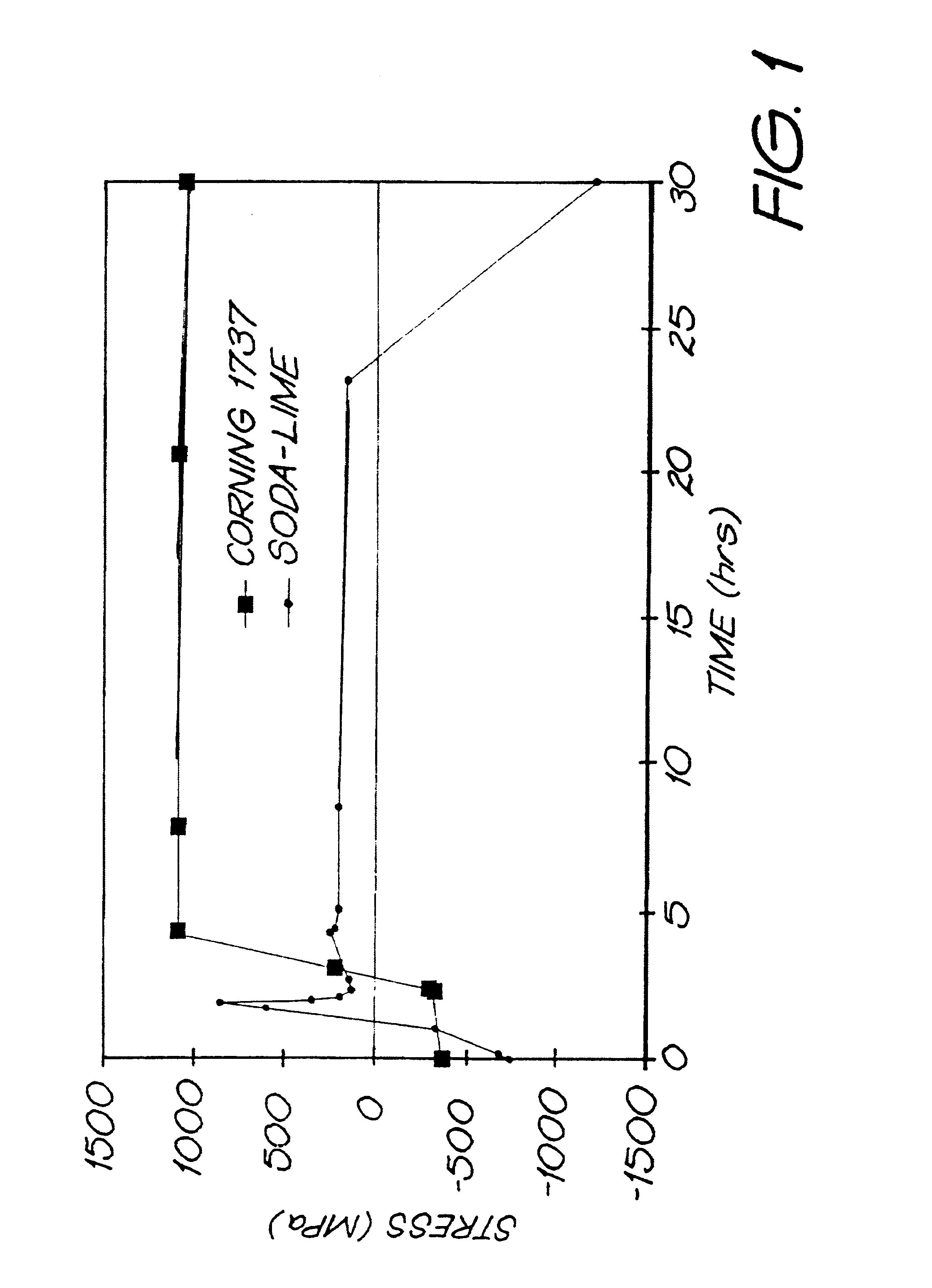
The invention will now be described in detail with specific examples using soda lime glass and with reference to Corning 1737 glass by way of comparison, however the invention is equally applicable to other low temperature glasses.

Normal Sequence

For polycrystalline silicon active matrix liquid crystal displays, silicon is normally deposited in amorphous form onto a high strain point glass substrate such as Corning 1737. The amorphous silicon is then crystallised without exceeding the temperature of the strain point of the glass either by prolonged heating at low temperature in a furnace or with very short high intensity pulses from a light source such as a laser which result in minimal heating of the glass. Sometimes both of these steps are applied sequentially. The resulting polycrystalline material is then processed into the desired electronic device. By minimising the thermal expansion difference between the glass and the silicon, stresses due to thermal expansion mismatch can be...


PUM

PropertyMeasurementUnit
Lengthaaaaaaaaaa
Percent by massaaaaaaaaaa

Abstract

A method of crystallizing amorphous silicon on a glass substrate relies on deliberately heating the glass substrate above its strain point during processing, making low temperature glasses, such as soda lime glasses, ideal for such use. Since the glass is plastic above this temperature while the silicon remains elastic, the glass is forced to conform to the shape defined by the silicon once this temperature is exceeded. This process relaxes any stresses which might otherwise be created in the glass or film, as long as the glass temperature is above the strain point. As the glass temperature is reduced back below the strain point, the glass becomes progressively more rigid and stresses will begin to build up in the film and glass. When cooled slowly, the stress in the film and the glass can be controlled by appropriate selection of a thermal expansion coefficient of the glass relative to that of silicon, particularly those with linear expansion coefficients in the range 4-10 ppm / ° C. below the strain point.

Description

The present invention relates generally to the field of semiconductor devices and in particular the invention provides an improved method for the formation of crystalline films on glass substrates.Considerable attention internationally is being directed towards developing technology for depositing polycrystalline silicon films on glass. This interest arises from the use of these films for forming electronic devices and circuits for active matrix liquid crystal displays and for use of these films in solar cells. Silicon film thickness could be in the 30 nm to 100 .mu.m range depending on application. For solar cell use, silicon film thickness in the 0.5-100 .mu.m range is of particular interest, with optimal designs likely to be in the 1-5 .mu.m range.As part of these efforts, considerable attention is being directed to the development of supporting glass substrates with specific properties, particularly in relation to the thermal expansion coefficient of the glass relative to silico...

Claims


Application Information

Patent Timeline
IPC IPC(8): C03C17/23C03C17/245C03C17/34C30B25/18C30B1/02C30B1/00H01L21/20H01L21/02H01L31/0392H01L31/036H01L31/18C03C17/22H01L31/04C30B25/00C30B28/02C30B29/06C30B33/02H01L21/84
CPCC03C17/245C03C17/3435C03C17/3482C30B1/02C30B25/18H01L31/03921C30B29/06H01L21/02422H01L21/0243H01L21/02524H01L21/02587H01L31/03682H01L31/1872C03C2217/282Y02E10/546Y02P70/50
Inventor GREEN, MARTIN ANDREWSHI, ZHENGRONGBASORE, PAUL ALANJI, JINGJIA
Owner CSG SOLAR AG
Why Eureka
Try Eureka