
Method for propagating switching activity information in digital combinatorial networks

a combinatorial network and switching activity technology, applied in stochastic cad, cad techniques, instruments, etc., can solve the problems of difficult to apply conventional methods for propagating signal and switching probabilities at inputs into logic circuits in practice for computing power consumed in logic circuits, and the primary source of power consumption is "dynamic power,

Inactive Publication Date: 2003-08-26
GOOGLE LLC
View PDF2 Cites 11 Cited by
  • Summary
  • Abstract
  • Description
  • Claims
  • Application Information

AI Technical Summary

Benefits of technology

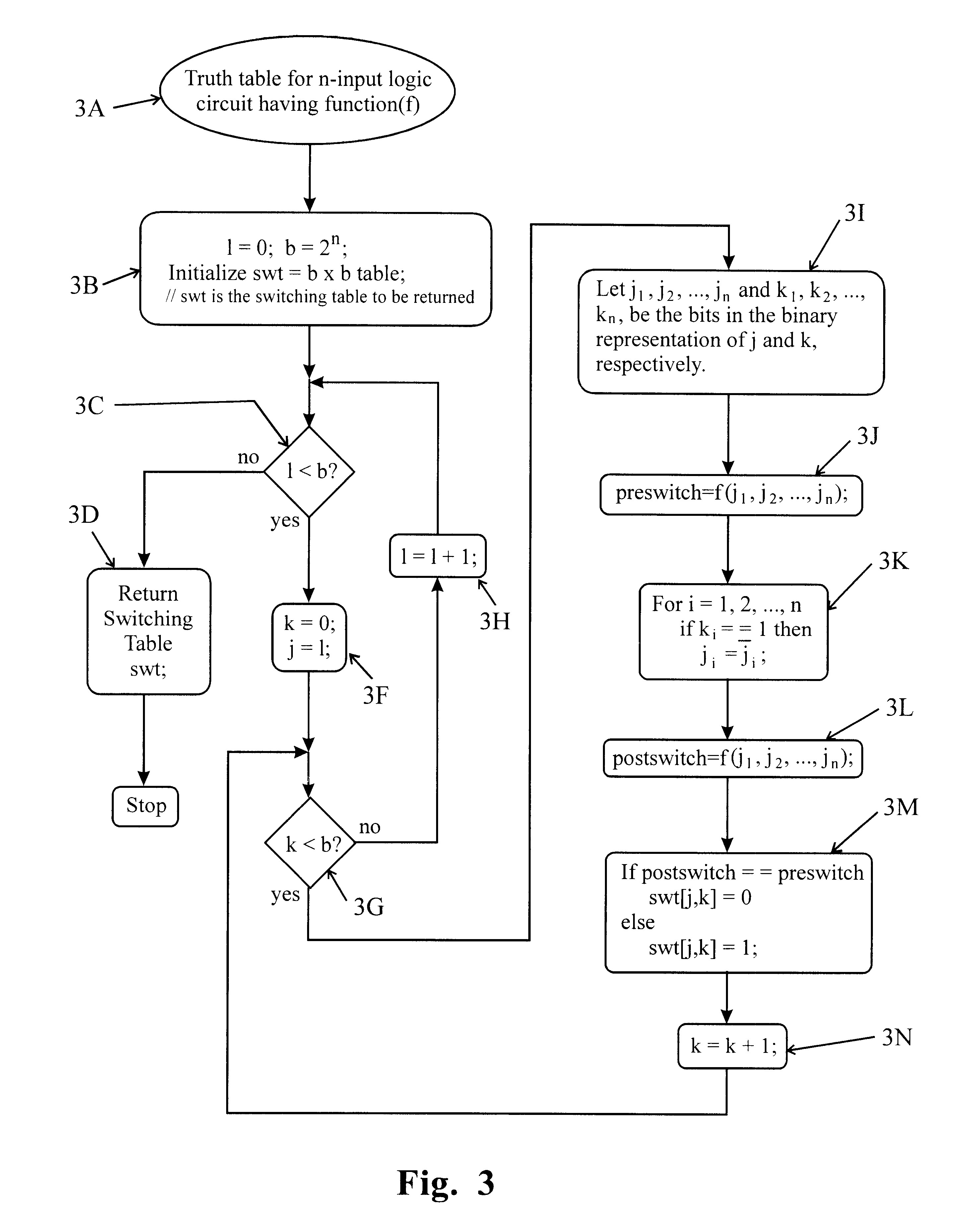
The present invention also provides a method of computing a signal probability at the output of the circuit. The method includes steps of creating a truth table for the circuit in accordance with the predetermined function, the truth table having entries respectively corresponding to signals at the inputs, choosing in sequence one of entries each of which has a predetermined value representing that a signal at the output of the circuit switches, determining whether a signal at one of the inputs corresponding to the entry chosen is at logic high, assigning to the signal at the one of the input...

Problems solved by technology

For CMOS devices, a primary source of power consumption is "dynamic power".
However, the conventional methods for propagating signal and switching probabilities at inputs into a logic circuit are difficult to apply in practice for computing power consumed in the logic circuit.
Such a simulation is a time consuming and costly process.
The Markov based process or the Boolean difference based process leads to highly complex computations in implementing the propagation of signal and switching probabilities.

Method used


Image

  • Method for propagating switching activity information in digital combinatorial networks
  • Method for propagating switching activity information in digital combinatorial networks
  • Method for propagating switching activity information in digital combinatorial networks

Examples


Embodiment Construction

Detailed illustrative embodiments of the present invention are disclosed herein. However, specific structural and functional details disclosed herein are merely representative for purposes of describing preferred embodiments of the present invention.

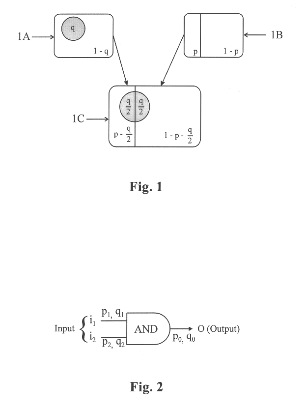
The present invention provides a method for computing signal and switching probabilities at output of a combinatorial logic circuit given signal statistics at inputs of the circuit. The method according to the present invention facilitates it to make an abstraction of switching activities of a logic circuit, to propagate switching activity information through the logic circuit, estimate various quality measures pertaining to power, testability and reliability, and to optimize design of the logic circuit for the estimated quality measures.

When a combinatorial logic circuit (e.g., Boolean function network) includes multiple logic circuits (e.g., logic operators) each of which has its own Boolean function, propagation of signal and switchin...


PUM


Abstract

A method is provided for computing signal and switching probabilities at an output of a logic circuit in a network having multiple logic circuits. The method for computing the signal and switching probabilities includes steps of creating a truth table for a logic circuit where the truth table has entries respectively corresponding to signals at inputs of the logic circuit, choosing in sequence one of entries each representing switching of a signal at the output of the circuit, determining whether a signal at an input corresponding to the chosen entry is at logic high, assigning an event probability representing that the signal is at logic high, and accumulating event probabilities respectively assigned to signals at inputs corresponding to the chosen entries to produce the signal probability at the output of the circuit.

Description

1. Field of the InventionThe present invention relates to a method for propagating switching activity information in a digital network, and more particularly to a method for computing and propagating signal and switching probabilities through components in a combinatorial logic circuit.2. Description of the Related ArtIn electronic systems, power consumption is one of the factors determining efficiency and functionality of the system. With the proliferation of wireless and hand-held electronic devices such as palm top computers, cellular telephones, etc., power consumption has become an important factor to be considered in designing and manufacturing such electronic devices. Since power consumption of such electronic devices directly relates to battery size and duration of usage of the devices between charges, battery life has become one of the most important factors in such electronic devices.To choose a battery for an electronic device, the expected power consumption of the electr...

Claims


Application Information

Patent Timeline
IPC IPC(8): G06F17/50
CPCG06F17/5022G06F2217/10G06F2217/78G06F2111/08G06F30/33G06F2119/06
Inventor NARASIMHAN, JAGANNATHANFARRAHI, AMIR
Owner GOOGLE LLC
Learn More