Metal gate electrode using silicidation and method of formation thereof

Inactive Publication Date: 2003-07-29
ADVANCED MICRO DEVICES INC
View PDF6 Cites 50 Cited by
  • Summary
  • Abstract
  • Description
  • Claims
  • Application Information

AI Technical Summary

Problems solved by technology

Furthermore, smaller transistors typically have lower turn on threshold voltages and faster switching speeds and consume less power in their operation.
As semiconductor transistors are scaled to reduce their dimensions, a number of problems have been presented.
For example, use of a very thin gate dielectric causes high gate current leakage, which diminishes device performance.
This very high concentration of dopant in the channel decreases current drive and can lead to undesirable drain-to-channel tunneling current.
Furthermore, use of polysilicon gate technology, as is typical, carries with it additional problems.
For example, polysilicon gates tend to suffer from polysilicon depletion or boron penetration effects, causing degradation in performance.
However, proposed processes typically involve deposition of metal instead of polysilicon, requiring complex process integration schemes.

Method used


Image

  • Metal gate electrode using silicidation and method of formation thereof
  • Metal gate electrode using silicidation and method of formation thereof
  • Metal gate electrode using silicidation and method of formation thereof

Examples


Embodiment Construction

Reference is now made in detail to specific embodiments of the present invention which illustrate the best mode presently contemplated by the inventors for practicing the invention.

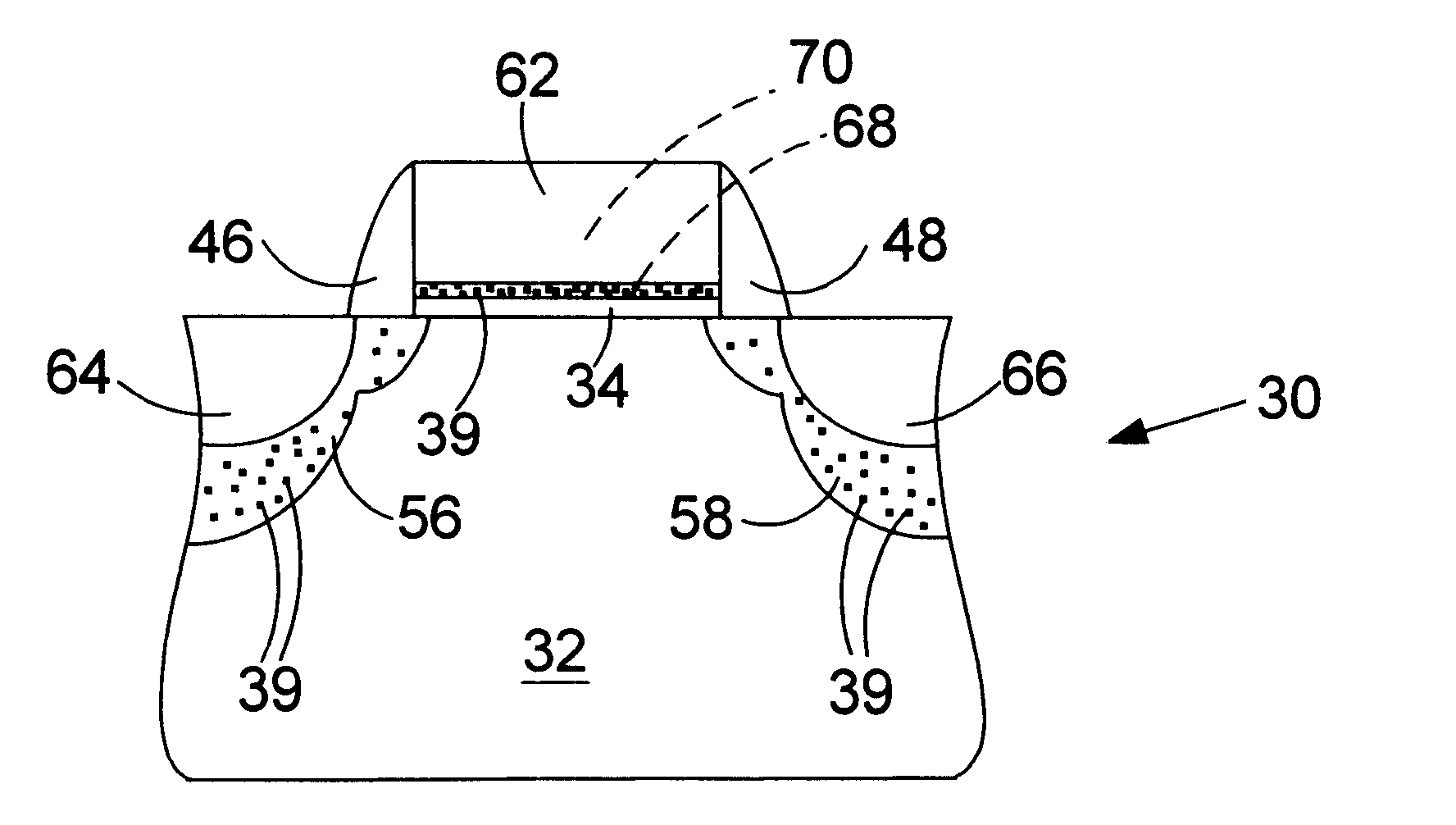
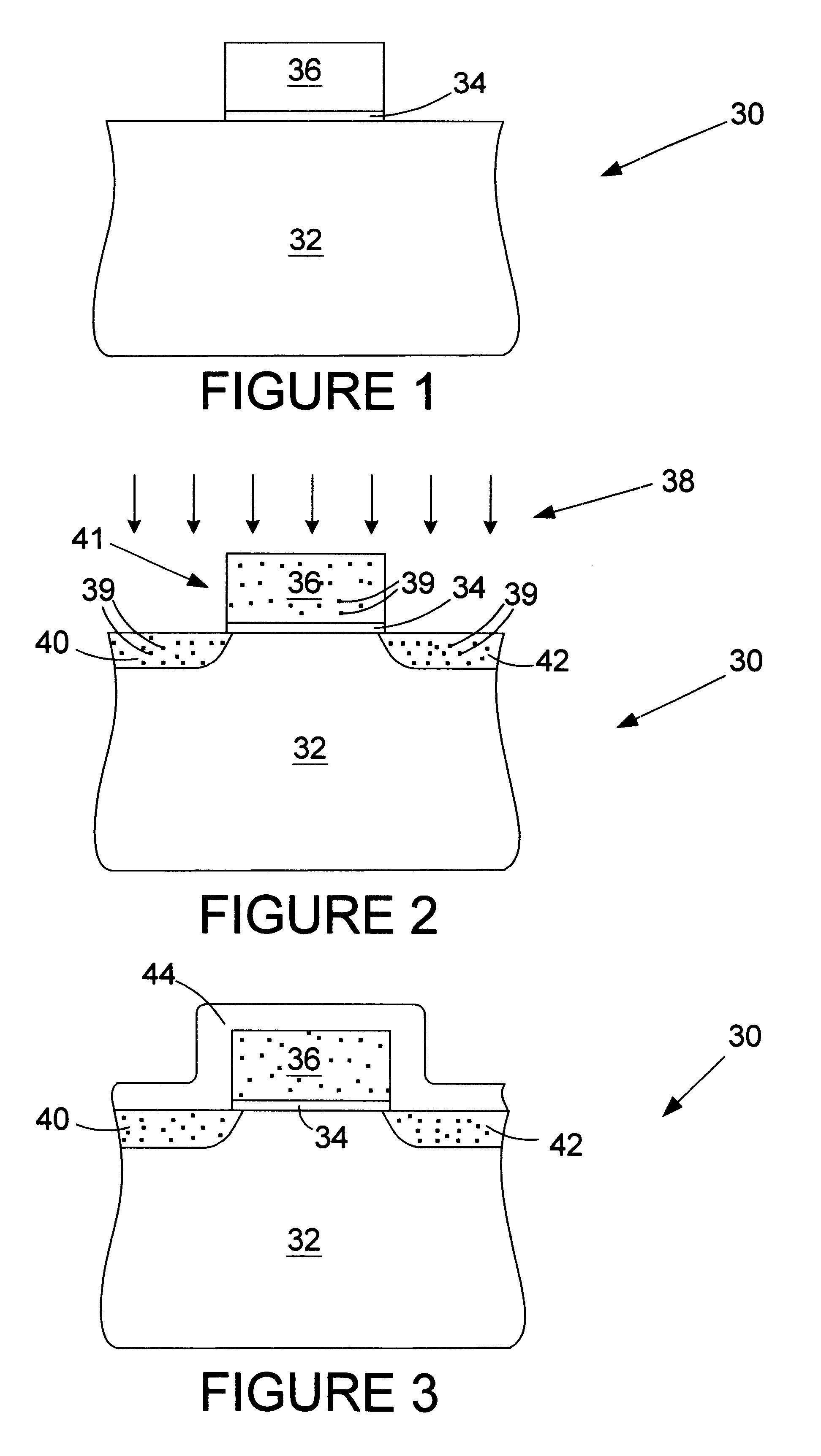
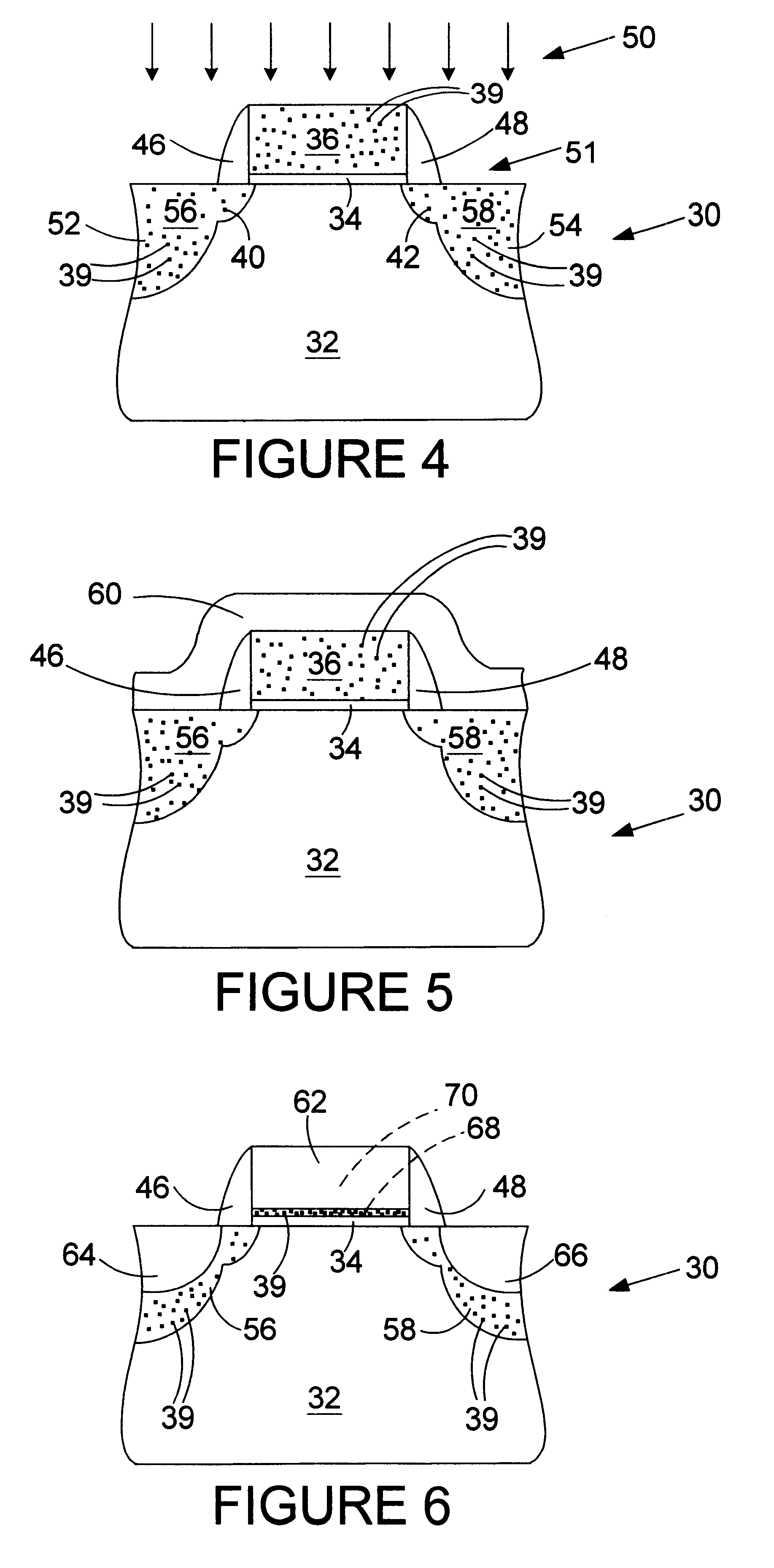
FIG. 1 illustrates a semiconductor device 30 including a silicon substrate 32 having formed thereon a dielectric in the form of a gate oxide 34, which in turn has thereon a polysilicon body 36, as is well known. An ion implantation 38 is undertaken (FIG. 2), using for example arsenic for an N type device, or boron for a P type device, so that ions 39 are implanted in the .silicon substrate 32 (using the polysilicon body 36 and the oxide 34 as an overall mask 41) to form lightly doped regions 40, 42 in the substrate 32, and in the polysilicon body 36. For an N type device, the dopant specie arsenic may be implanted at an energy level of for example 3 keV and a dosage level of for example 1 el5 cm.sup.2, while for a P type device, the dopant specie boron may be implanted at an energy level of for example 4 ...


PUM


Abstract

A semiconductor device is fabricated by providing a substrate, and providing a dielectric layer on the substrate. A polysilicon body is formed on the dielectric layer, and a metal layer is provided on the polysilicon body. A silicidation process is undertaken to silicidize substantially the entire polysilicon body to form a gate on the dielectric. In an alternative process, a cap layer is provided on the polysilicon body, which cap layer is removed prior to the silicidation process. The polysilicon body is doped with a chosen specie prior to the silicidation process, which dopant, during the silicidation process, is driven toward the dielectric layer to form a gate portion having a high concentration thereof adjacent the dielectric, the type and concentration of this specie being instrumental in determining the work function of the formed gate.

Description

1. Technical FieldThis invention relates generally to semiconductor technology, and more particularly, to semiconductor devices which incorporate a silicidation process.2. Background ArtA common trend in modern integrated circuit manufacture is to produce transistors having feature sizes as small as possible. To achieve a high density integrated circuit, features such as the conductors, source and drain junctions, and interconnections to the junctions must be made as smallest possible. As feature sizes decrease, the sizes of the resulting transistors as well as the interconnections between transistors also decrease. Having smaller transistors allows more transistors to be placed on a single monolithic substrate. Accordingly, relatively large circuits can be incorporated on a single and relatively small die area. Furthermore, smaller transistors typically have lower turn on threshold voltages and faster switching speeds and consume less power in their operation. These features, in co...

Claims


Application Information

Patent Timeline
IPC IPC(8): H01L21/285H01L21/28H01L21/02H01L29/49H01L29/40H01L21/336H01L29/423H01L29/78
CPCH01L21/28097H01L21/28518H01L29/4975H01L29/6659H01L29/665H01L29/66545H01L21/18H01L21/24
Inventor MASZARA, WITOLDKRIVOKAPIC, ZORAN
Owner ADVANCED MICRO DEVICES INC
Why Eureka
Try Eureka