Article comprising a multimode optical fiber coupler
a multi-mode optical fiber and coupler technology, applied in the direction of instruments, bundled fibre light guides, active medium shape and construction, etc., can solve the problems of loss in the transmission of light that travels from one device to the other, loss in the making of waveguide connections, and inherently produced loss of optical communication systems between the various system components. to achieve the effect of efficient couple between waveguides
- Summary
- Abstract
- Description
- Claims
- Application Information
AI Technical Summary
Benefits of technology
Problems solved by technology
Method used
Image
Examples
example 1
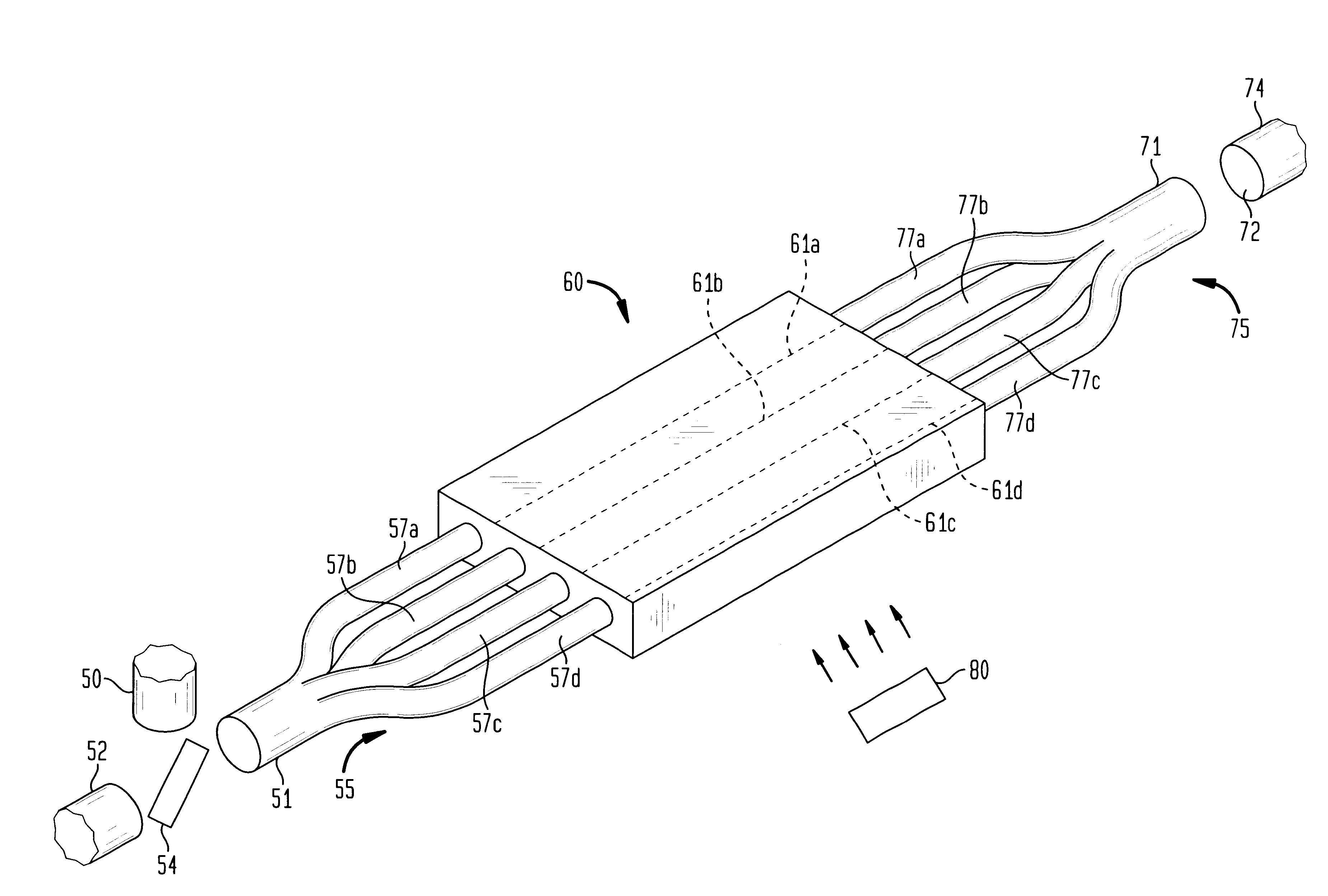
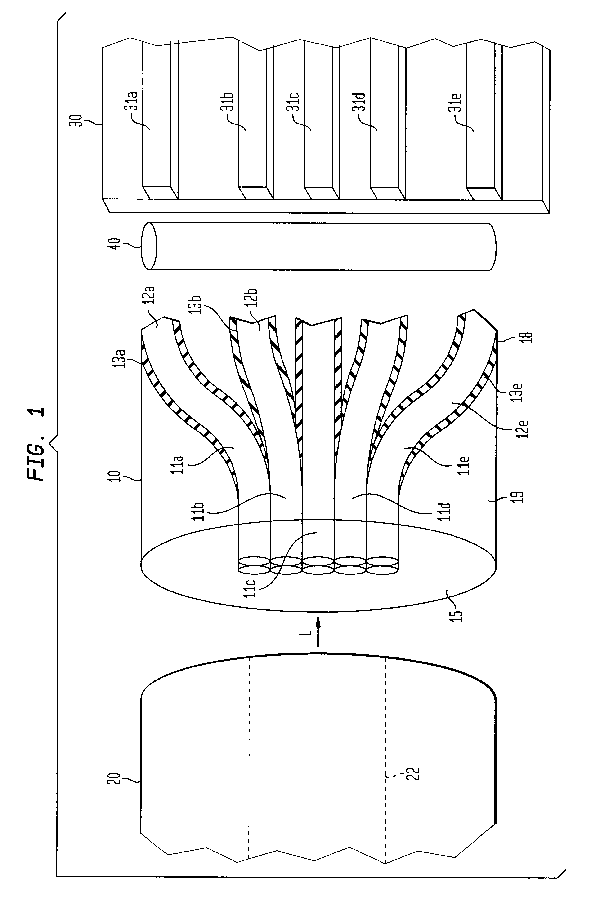
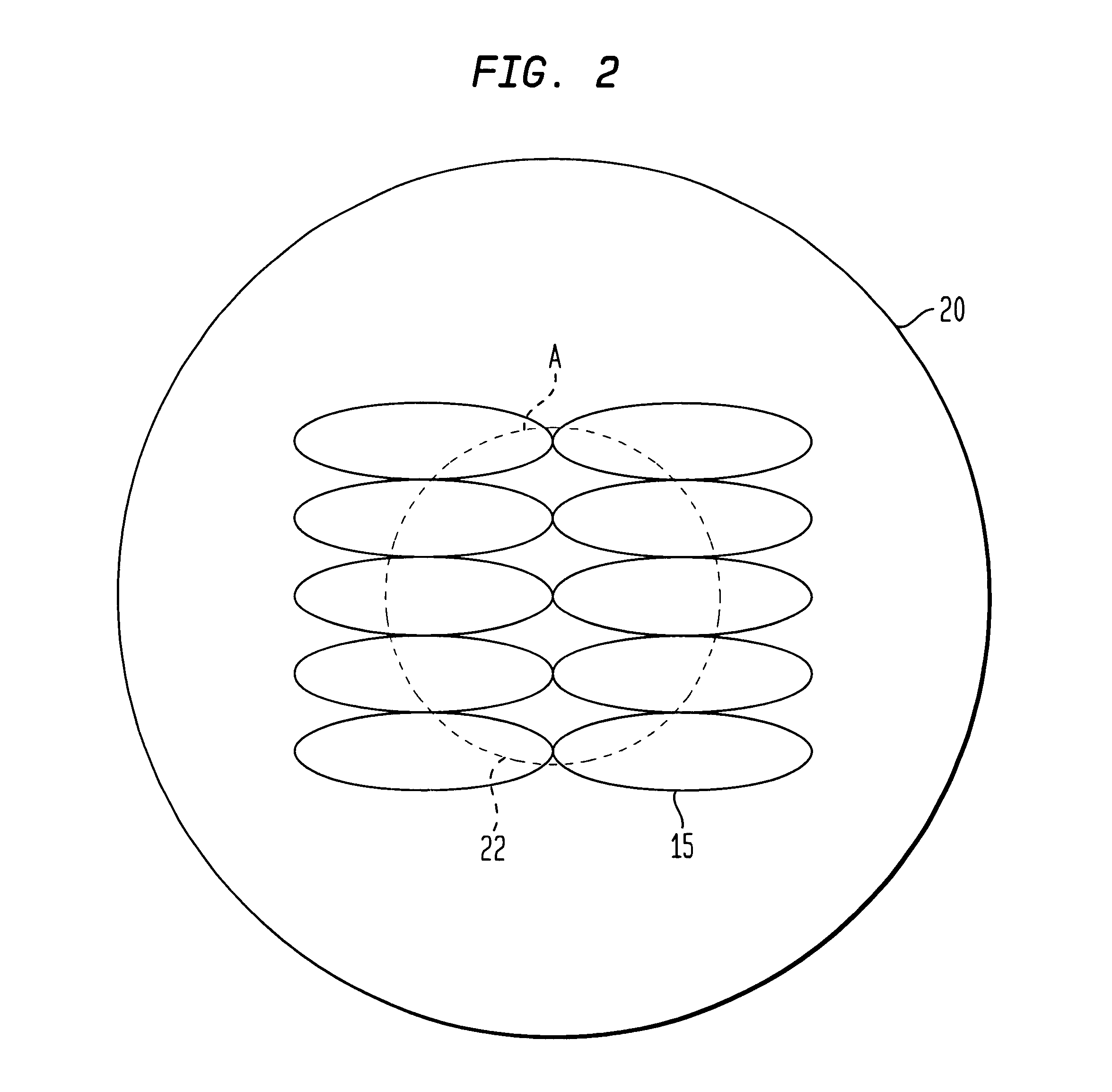
A multimode input fiber having a core of .about.50 .mu.m is coupled to an array of waveguides each having a height (film thickness) of 3 .mu.m at the input end. The array of waveguides comprise aluminosilicate having a NA of 0.67. Optical fibers used for the coupling device have a NA of 0.23, and thus, the desired ratio of fiber diameter to waveguide height is 0.67 / 0.23.about.3. The diameter of the optical fibers is thus 9 .mu.m (waveguide height of 3 .mu.m.times.3), and nine fibers are needed to cover the 50 .mu.m input core area of the multimode input fiber. (A greater number of fibers, i.e., 30, could be needed if the fibers are round.) Advantageously, at the input end the planar waveguides have a width of 30 .mu.m and taper down to a dimension of 10 .mu.m.times.3 .mu.m to take advantage of the lateral dimension of the higher NA of the planar waveguide, as compared to the fiber.
example 2
A solid taper at the output end of the multimode collection fiber dimension reduces the NA requirements of the optical fibers in the coupler as compared with the configuration in Example 1. The output end of the multimode collection fiber is tapered from 50 .mu.m to 100 .mu.m which drops the NA requirement of the fibers in the bundle from 0.23 to 0.23(2).sup.1 / 2 =0.16. Thirty-two fibers of the same elongated cross-section of Example are needed, but signals may be transmitted to a waveguide planar waveguide having a smaller height (film thickness) of 2.1 .mu.m (9.times.0.16 / 0.67=2.1). The lateral dimension of the planar waveguide is tapered down to 6.5 .mu.m, resulting in planar waveguide dimensions of 2.1.times.6.5 .mu.m, to support less modes as compared with Example 1.
PUM
 Abstract
Description
Claims
Application Information
 - R&D
- Intellectual Property
- Life Sciences
- Materials
- Tech Scout
- Unparalleled Data Quality
- Higher Quality Content
- 60% Fewer Hallucinations
Browse by: Latest US Patents, China's latest patents, Technical Efficacy Thesaurus, Application Domain, Technology Topic, Popular Technical Reports.
© 2025 PatSnap. All rights reserved.Legal|Privacy policy|Modern Slavery Act Transparency Statement|Sitemap|About US| Contact US: help@patsnap.com


