
Decontamination of a plasma reactor using a plasma after a chamber clean

a plasma reactor and plasma technology, applied in the direction of solid-state diffusion coating, mechanical control devices, process and machine control, etc., can solve the problems of cvd layer deposition rate, metal layer damage, precursor absorption,

Inactive Publication Date: 2002-09-10
APPLIED MATERIALS INC
View PDF22 Cites 63 Cited by
  • Summary
  • Abstract
  • Description
  • Claims
  • Application Information

AI Technical Summary

Problems solved by technology

The high temperatures at which some thermal CVD processes operate can damage device structures having metal layers previously formed thereon.
The presence of fluorine or other sorbable contaminants may affect the absorption of precursors and slow or inhibit the deposition rate of the CVD layer.
Addition of nitrogen to the process gas may further block the passage of contaminants through the PECVD layer.

Method used


Image

  • Decontamination of a plasma reactor using a plasma after a chamber clean
  • Decontamination of a plasma reactor using a plasma after a chamber clean
  • Decontamination of a plasma reactor using a plasma after a chamber clean

Examples


Embodiment Construction

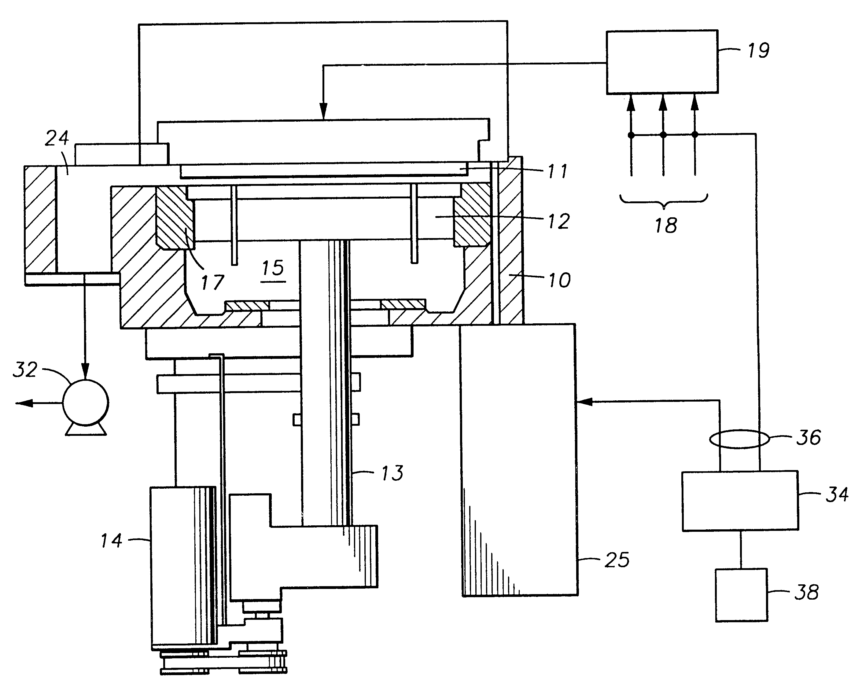
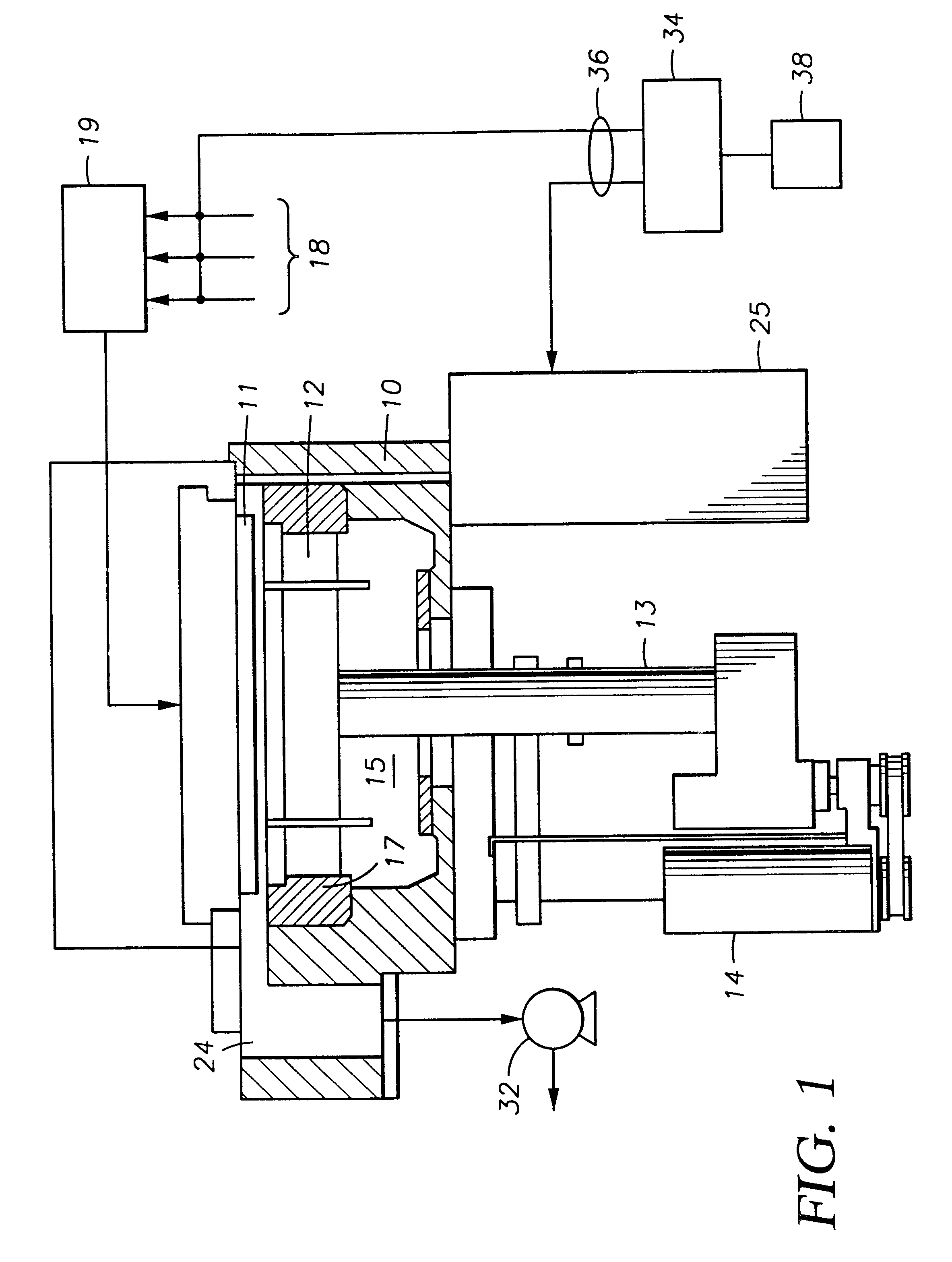
The following example demonstrates the present invention by describing a successful pretreatment of a CVD plasma reactor. This example was undertaken using a chemical vapor deposition chamber, and in particular, a "CENTURA DxZ" plasma reactor fabricated and sold by Applied Materials, Inc., Santa Clara, Calif.

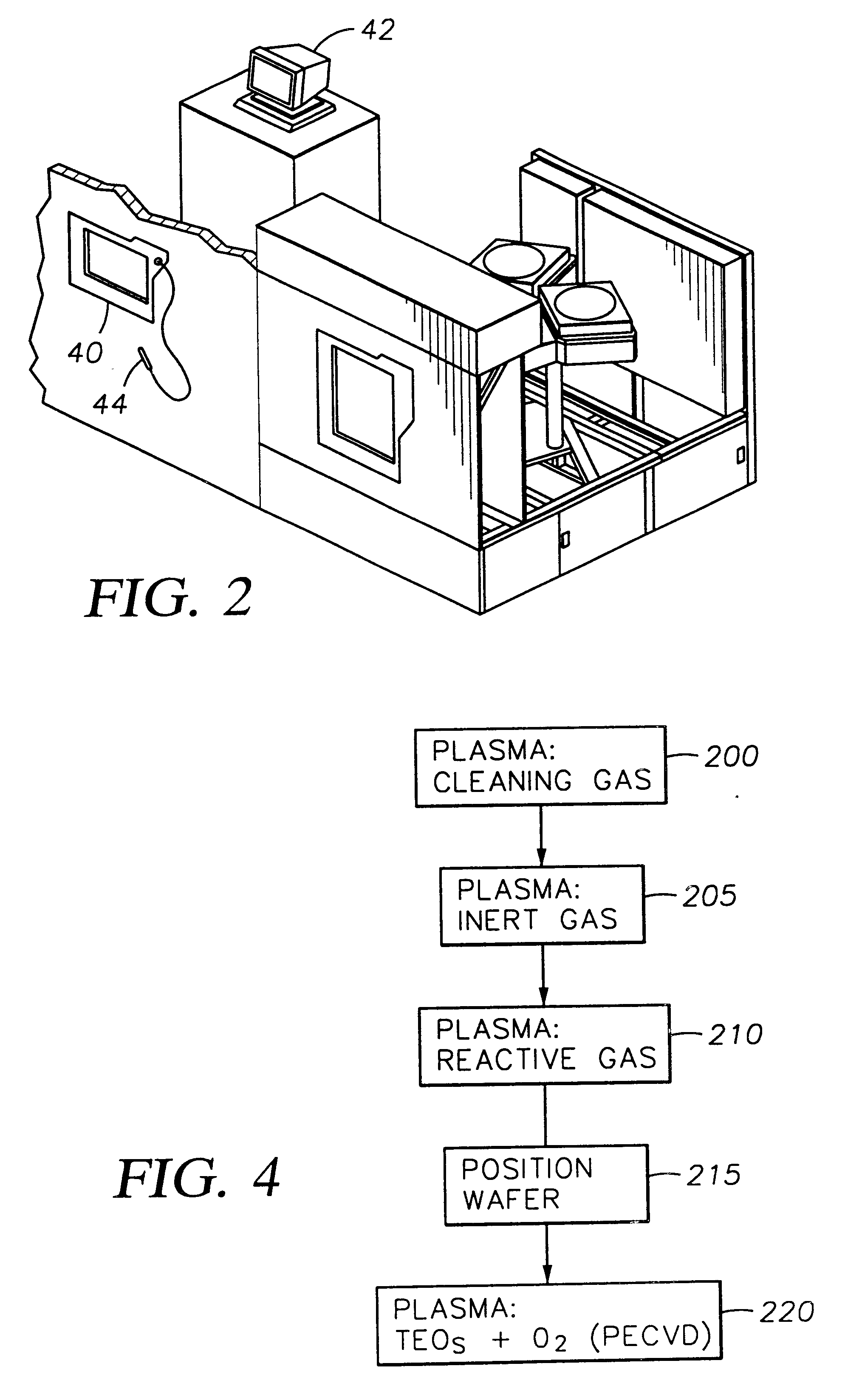
The chamber was stabilized for 5.0 seconds at a pressure of 4.4 Torr with an oxygen flow of 550 sccm, a hexafluoroethylene (C.sub.2 F.sub.6) flow of 400 sccm, and a nitrogen trifluoride (NF.sub.3) flow of 60 sccm prior to raising of the susceptor and prior to application of RF power. The chamber was then cleaned for 55.0 seconds by applying 1950 W of RF power (13.56 MHZ) to the gas distribution plate while the grounded susceptor remained in the fully lowered position. The susceptor was then raised to 280 mil separation from the gas distribution plate and the contaminants where cleaned from the chamber for 30.0 seconds with a helium plasma at a pressure of 3.0 Torr after shutting...


PUM

PropertyMeasurementUnit
temperatureaaaaaaaaaa
volumeaaaaaaaaaa

Abstract

A method and apparatus for reducing fluorine and other sorbable contaminants in plasma reactor used in chemical vapor deposition process such as the deposition of silicon oxide layer by the reaction of TEOS and oxygen. According to the method of the present invention, plasma of an inert gas is maintained in plasma reactor following chamber clean to remove sorbable contaminants such as fluorine. The plasma clean is typically followed by seasoning of the reactor to block or retard remaining contaminants. According to one embodiment of the invention, the combination of chamber clean, plasma clean, and season film is conducted before PECVD oxide layer is deposited on wafer positioned in the plasma reactor.

Description

1. Field of the InventionThe present invention relates to the fabrication of integrated circuits. More particularly, the invention provides a cleaning technique for a plasma chamber utilized in the manufacture of integrated circuits.2. Background of the InventionOne of the primary steps in the fabrication of modern semiconductor devices is the formation of a thin film on a semiconductor substrate by chemical reaction of gases. Such a deposition process is referred to as chemical vapor deposition or CVD. Conventional thermal CVD processes supply reactive gases to the substrate surface where heat-induced chemical reactions take place to produce a desired film. The high temperatures at which some thermal CVD processes operate can damage device structures having metal layers previously formed thereon.Processes which have been developed to deposit insulation films over metal layers at relatively low temperatures include plasma-enhanced CVD (PECVD) techniques such as described in U.S. Pat...

Claims


Application Information

Patent Timeline
Patent Type & Authority Patents(United States)
IPC IPC(8): B08B7/00C23C16/44
CPCB08B7/0035C23C16/4405H01J37/32862Y10T29/413Y10T29/41Y10T29/417
Inventor GUPTA, ANAND
Owner APPLIED MATERIALS INC
Learn More