Cleaning method
- Summary
- Abstract
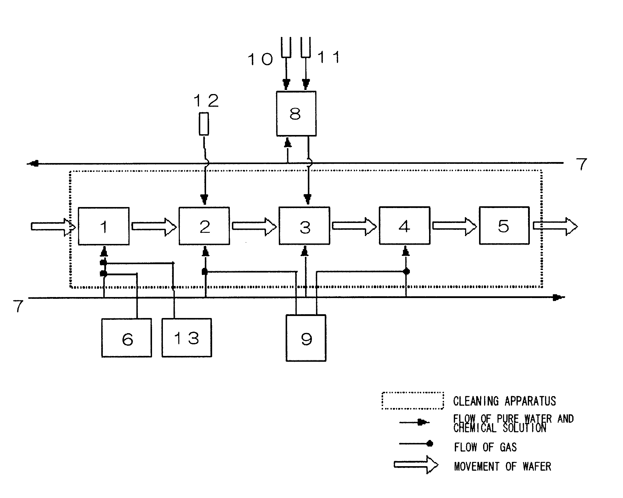
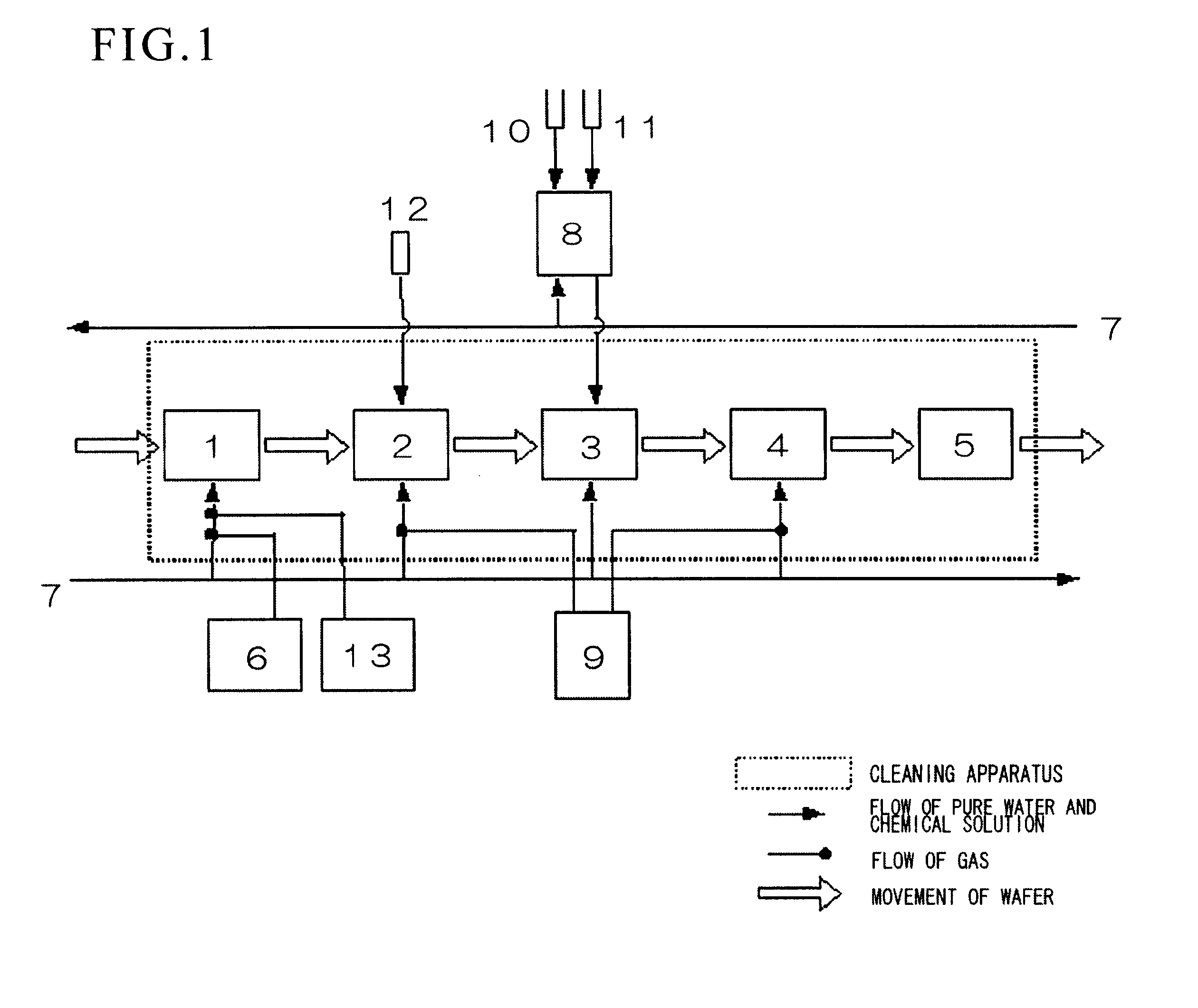
- Description
- Claims
- Application Information
AI Technical Summary
Benefits of technology
Problems solved by technology
Method used
Image

Examples
embodiment 1
For the purposes of comparison, the organic materials, metals, and microparticles present on wafer surfaces and the flatness of the surfaces were measured in a manner identical to that of embodiment 1 after cleaning using conventional methods. The results thereof are shown in Table 1.
The cleaning conditions in these comparative examples were as shown below; and the mixing ratios of the chemicals and chemical solutions employed and the cleaning times are as given below.
1: Sulfuric acid / hydrogen peroxide cleaning
120.degree. C., 10 minutes
Sulfuric acid (97 wt %): hydrogen peroxide (30 wt %)=4:1
2: Ultrapure water rinse
25.degree. C., 10 minutes
3: Dilute hydrofluoric acid cleaning
25.degree. C., 1 minute
Hydrofluoric acid concentration: 0.5 wt %
4: Ultrapure water rinse
25.degree. C., 10 minutes
5: Ammonia / hydrogen peroxide cleaning
80.degree. C., 10 minutes
Ammonia (28 wt %): hydrogen peroxide (30 wt %): ultrapure water=1:1:5
6: Ultrapure water rinse
25.degree. C., 10 minutes
7: Hot ultrapure wate...
embodiment 2
The ozone concentration of the ozonated ultrapure water of the first process was changed to, respectively, 1 mg / L, 2 mg / L, 3 mg / L, and 5 mg / L, and the other cleaning conditions were the same as in embodiment 1, and this cleaning method was conducted.
After conducting cleaning with the cleaning method of this embodiment, the amount of organic material on the wafer surface was assessed using a Fourier transform infrared spectrometer (produced by Bio-Rad Corporation). The results thereof are shown in Table 2.
embodiment 3
The hydrogen concentration in the hydrogenated ultrapure water of the second process was altered to, respectively, 0 mg / L, 0.2 mg / L, 0.5 mg / L, and 1.0 mg / L, and the other cleaning conditions were as in embodiment 1, and this cleaning method was thus carried out.
After cleaning 8-inch n-type (100) silicon substrates having a resistivity within a range of 8-12 .OMEGA..multidot.cm using the method of the present embodiment, the number of microparticles on the surface of the wafers was assessed using a wafer surface foreign matter detection apparatus (produced by KLA.multidot.Tencor Corporation) The results thereof are shown in Table 3.
PUM
| Property | Measurement | Unit |
|---|---|---|
| Concentration | aaaaa | aaaaa |
| Concentration | aaaaa | aaaaa |
| Concentration | aaaaa | aaaaa |
Abstract
Description
Claims
Application Information
 - R&D
- Intellectual Property
- Life Sciences
- Materials
- Tech Scout
- Unparalleled Data Quality
- Higher Quality Content
- 60% Fewer Hallucinations
Browse by: Latest US Patents, China's latest patents, Technical Efficacy Thesaurus, Application Domain, Technology Topic, Popular Technical Reports.
© 2025 PatSnap. All rights reserved.Legal|Privacy policy|Modern Slavery Act Transparency Statement|Sitemap|About US| Contact US: help@patsnap.com