Magneto-optical recording method capable of adjusting the sizes magnetic domain
- Summary
- Abstract
- Description
- Claims
- Application Information
AI Technical Summary
Problems solved by technology
Method used
Image
Examples
embodiment 1
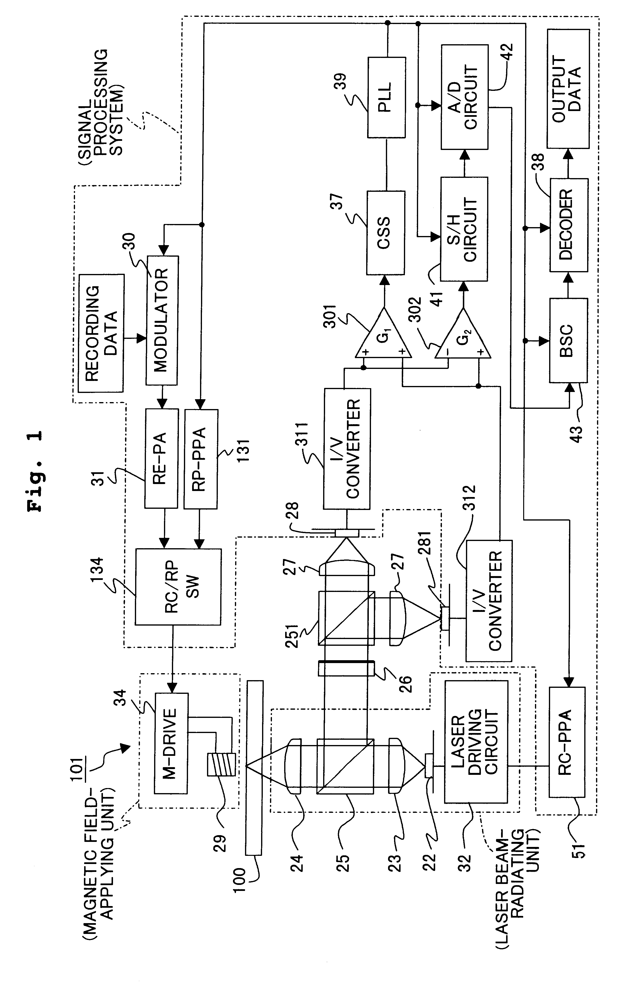
FIG. 1 schematically shows the structure of a recorder according to the invention. The recorder 101 consists mainly of a laser beam radiating unit for irradiating a magneto-optical recording medium 100 with a light beam pulsed in synchronism with coded data, a magnetic field applying unit for applying a controlled magnetic field to the recording medium 100 during recordation and reproduction, and a signal processing system for detecting and processing a signal from the recording medium 100. The laser beam radiating unit includes a laser 22, which is connected to a laser driving circuit 32 and a recording pulse width / phase adjusting circuit (RC-PPA) 51. The driving circuit 32 receives a signal from the adjusting circuit 51, and controls the laser pulse width and phase of the laser 22. The adjusting circuit 51 receives a clock signal, which will be described later on, from a PLL circuit 39, and generates a first synchronizing signal for adjusting the phase and pulse width of a recordi...
embodiment 2
In this embodiment, a recording method according to the eighth aspect of the invention will be described in detail. FIG. 10 typically shows the dependency of recorded magnetic domain shapes of magneto-optical discs on recording magnetic field strength. In FIG. 10, a disc A is a magneto-optical recording medium including a substrate of polycarbonate, a layer of silicon nitride which is 60 nm in thickness, a recording layer of TbFeCo which is 8 nm in thickness, a recording auxiliary layer of Pt.sub.84 Co.sub.16 which is 40 nm in thickness and a layer of silicon nitride which is 60 nm in thickness. The layers are stacked on the substrate. A disc B is a magneto-optical recording medium including a substrate of polycarbonate, a layer of silicon nitride which is 60 nm in thickness, a recording layer of TbFeCo which is 8 nm in thickness, a layer of silicon nitride which is 60 nm in thickness and a layer of Al alloy which is 50 nm in thickness. The layers are stacked on the substrate. FIG. ...
PUM
 Abstract
Description
Claims
Application Information
 - R&D
- Intellectual Property
- Life Sciences
- Materials
- Tech Scout
- Unparalleled Data Quality
- Higher Quality Content
- 60% Fewer Hallucinations
Browse by: Latest US Patents, China's latest patents, Technical Efficacy Thesaurus, Application Domain, Technology Topic, Popular Technical Reports.
© 2025 PatSnap. All rights reserved.Legal|Privacy policy|Modern Slavery Act Transparency Statement|Sitemap|About US| Contact US: help@patsnap.com


