
Electron beam dose control for scanning electron microscopy and critical dimension measurement instruments

a technology of scanning electron microscopy and critical dimension measurement, applied in the field of system and method of imaging specimens, can solve problems such as obscuring image features in that small area, and achieve the effect of reducing charge build-up

Inactive Publication Date: 2001-04-03
KLA TENCOR TECH CORP
View PDF5 Cites 29 Cited by
  • Summary
  • Abstract
  • Description
  • Claims
  • Application Information

AI Technical Summary

Benefits of technology

FIG. 8 shows a portion of an image on a specimen to illustrate the capability of multiple feature measurement of the present invention without having to reposition the specimen.
FIG. 9 illustrates a second embodiment of the present invention that minimizes the charge build-up in a specimen when being scanned.

Problems solved by technology

That excess charge causes an image of that small area to appear dark, thus obscuring image features in that small area.

Method used


Image

  • Electron beam dose control for scanning electron microscopy and critical dimension measurement instruments
  • Electron beam dose control for scanning electron microscopy and critical dimension measurement instruments
  • Electron beam dose control for scanning electron microscopy and critical dimension measurement instruments

Examples


Embodiment Construction

Reference will now be made in detail to the preferred embodiments of the present invention, examples of which are illustrated in the accompanying drawings.

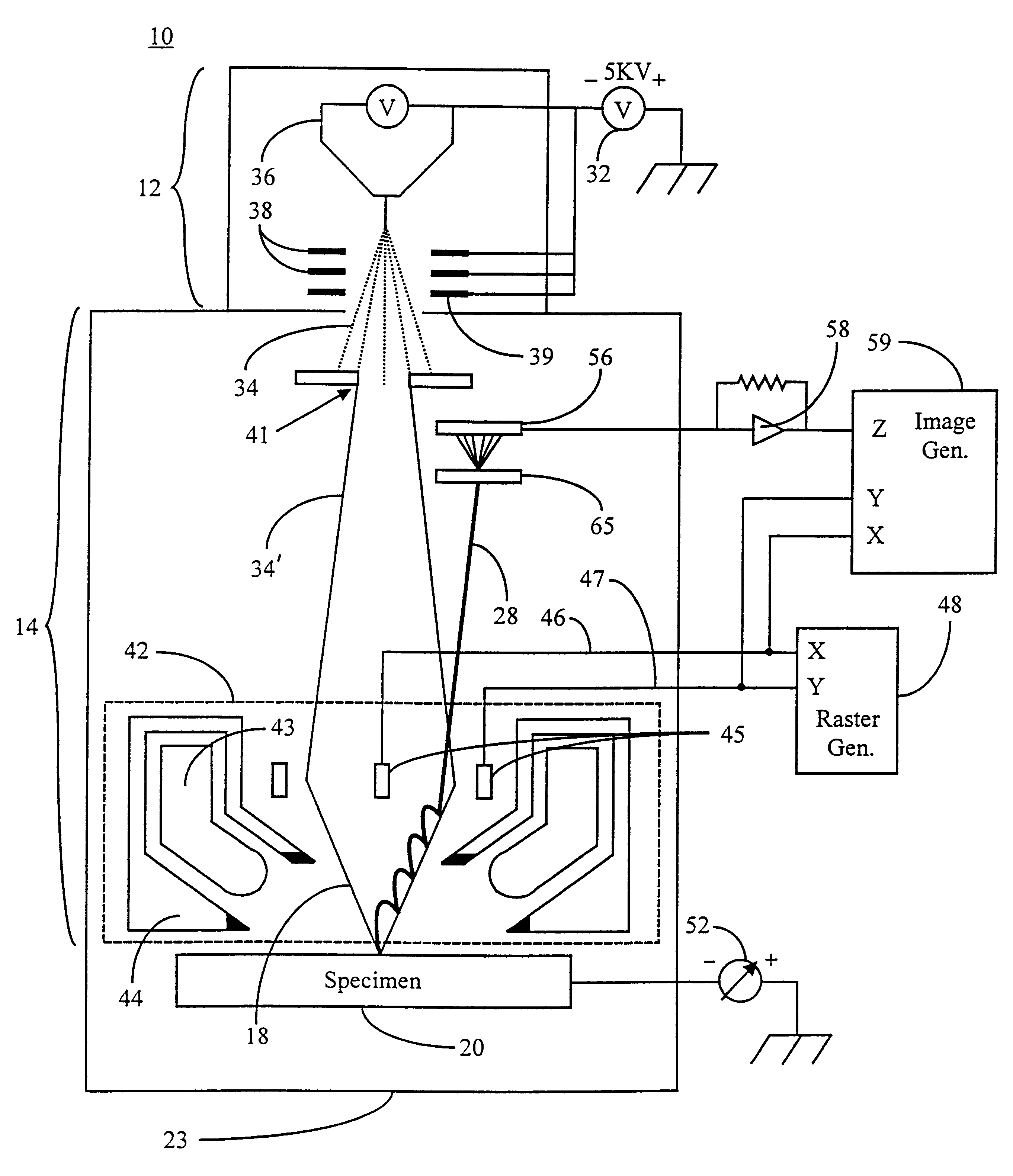
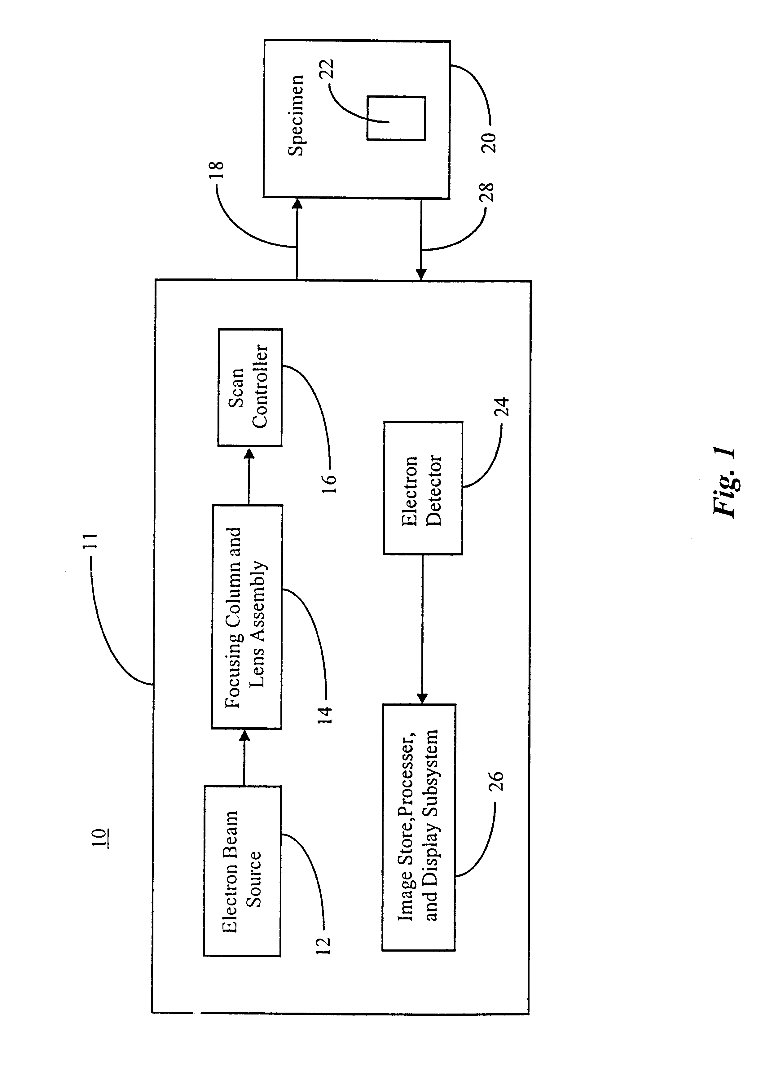
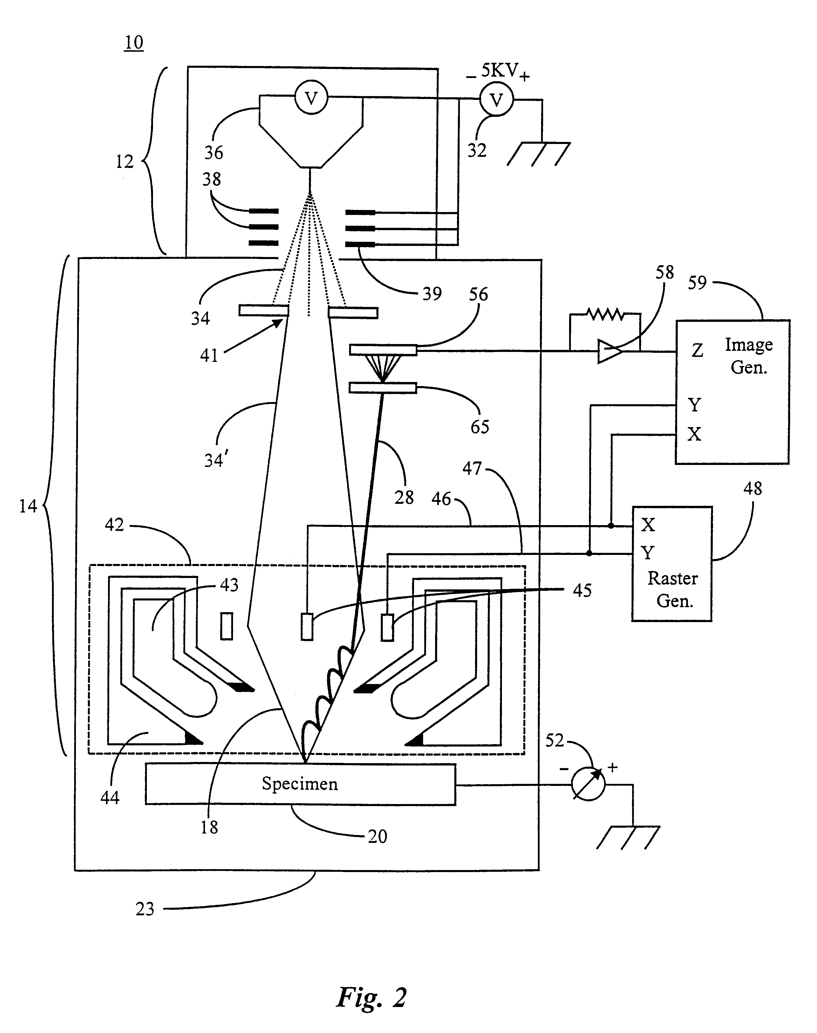
FIG. 1 shows a block diagram of system 10 including an electron microscope subsystem 11 of the present invention. The electron microscope subsystem 11 includes an electron beam source 12, a focusing column and lens assembly 14, and a scan controller 16 to scan an electron beam across selected regions of specimen 20. Also included in electron microscope system 11 is an electron detector 24 to detect secondary and backscattered electrons from specimen 20. In system 10 of the present invention, electron detector 24 is selected to have a bandwidth that is at least adequate to detect the secondary and backscattered electrons that form electron signal 28. For example, electron detector 24 may be a micro-channel plate, micro-sphere plate, semiconductor diode, or a scintillator / photomultiplier (PMT) assembly, each well known in the art. ...


PUM


Abstract

A system and method for controlling electron exposure on image specimens by adjusting a raster scan area in-between scan frame cycles. A small, zoomed-in, scan area and the surrounding area are flooded with positive charge for a number of frame cycles between scan frames to reduce the voltage differential between the scan area and surrounding area, thereby reducing the positive charge buildup which tends to obscure small features in scanned images. The peak current into a pixel element on the specimen is reduced by scanning the beam with a line period that is very short compared to regular video. Frames of image data may further be acquired non-sequentially, in arbitrarily programmable patterns. Alternatively, an inert gas can be injected into the scanning electron microscope at the point where the electron beam impinges the specimen to neutralize a charge build-up on the specimen by the ionization of the inert gas by the electron beam.

Description

The present invention relates generally to enhanced feature measurement in scanning electron microscopy, and more specifically to a system and methods for controlling electron exposure on image specimens in scanning electron metrology, particularly in the inspection of features of micro-circuits. It may also apply to critical dimension measurement in similar instruments.In scanning electron microscopy, a beam of electrons is scanned over a specimen, and the resulting electrons that are returned from the specimen surface are used to create an image of the specimen surface. In some systems, the beam is arbitrarily controllable to make multiple scan passes over specific areas or portions of areas at different sample frequencies to magnify the image of the surface.On a specimen made of a substantially insulative material (e.g., a semiconductor material), performing multiple scans over the same small area may cause the specimen to accumulate an excess positive charge in that small area r...

Claims


Application Information

Patent Timeline
Patent Type & Authority Patents(United States)
IPC IPC(8): H01J37/28H01J37/20H01J37/147
CPCH01J37/28H01J2237/004H01J2237/2817
Inventor RICHARDSON, NEILASKARY, FARIDCONCINA, STEFANO E.MONAHAN, KEVIN M.ADLER, DAVID L.
Owner KLA TENCOR TECH CORP
Learn More