
Separate output power supply to reduce output noise for a simultaneous operation

Inactive Publication Date: 2001-01-23
III HLDG 4
View PDF7 Cites 25 Cited by
  • Summary
  • Abstract
  • Description
  • Claims
  • Application Information

AI Technical Summary

Benefits of technology

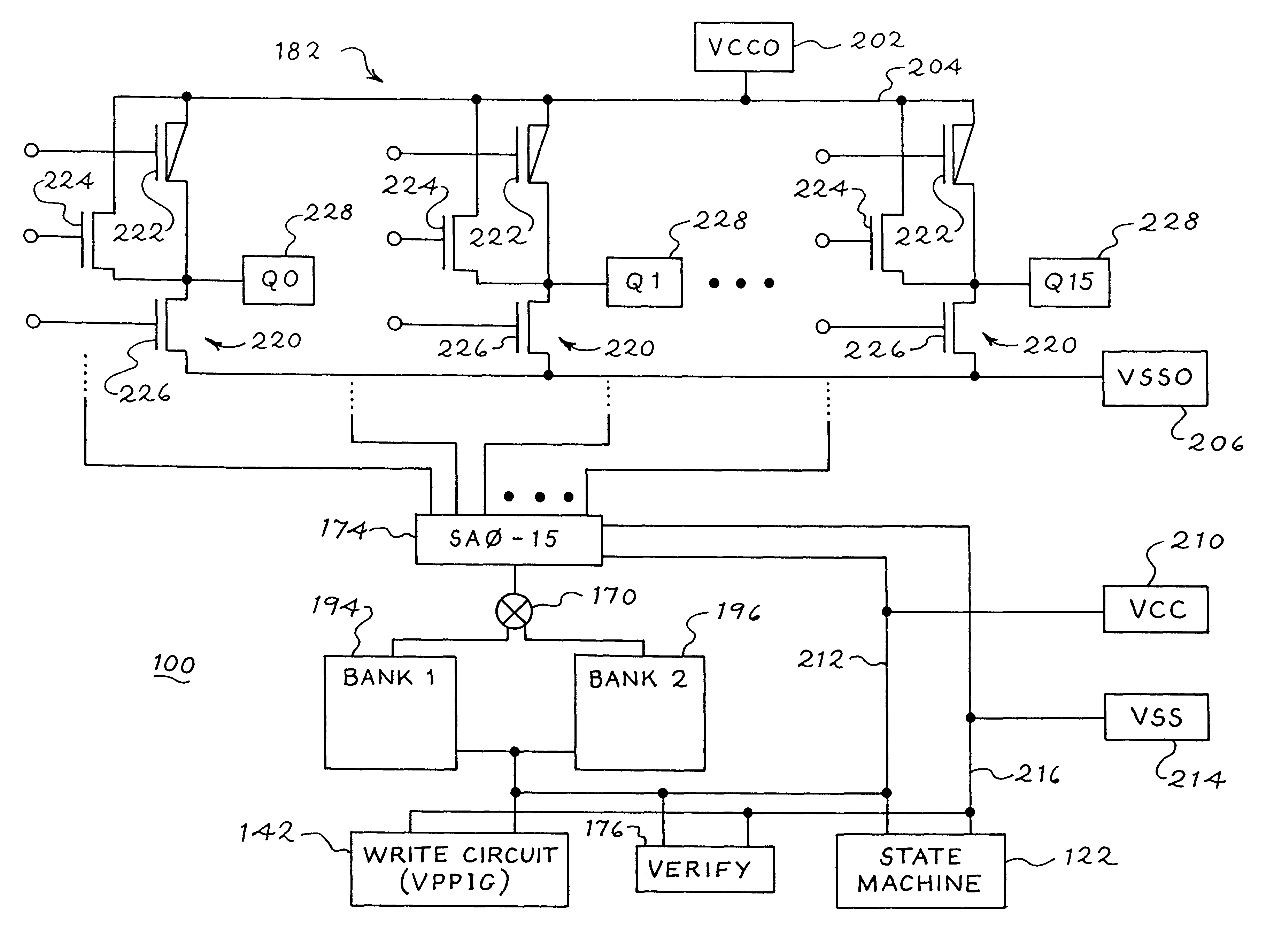
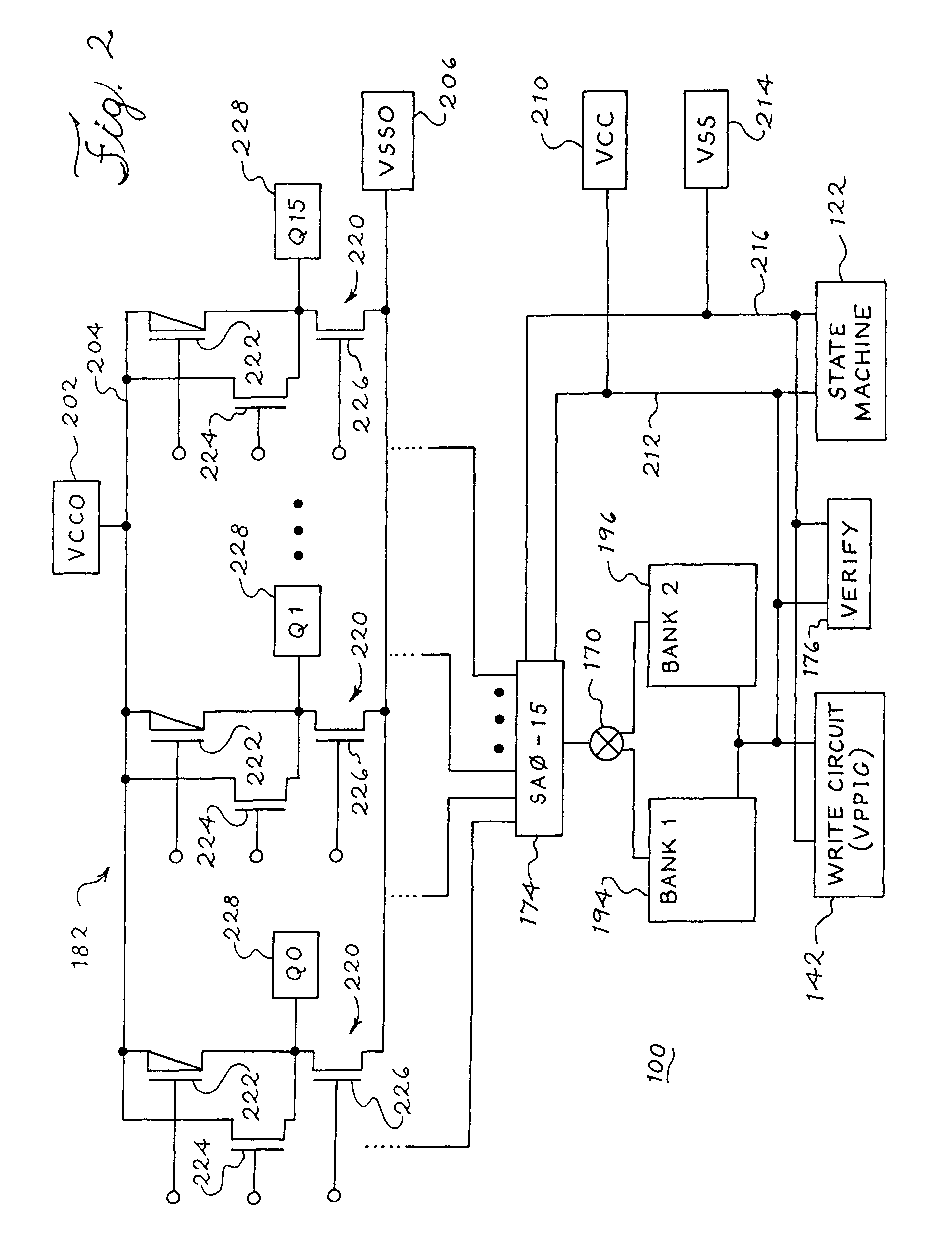
The present invention is defined by the following claims, and nothing in this section should be taken as a limitation on those claims. By way of introduction, the preferred embodiments described below relate to an improved simultaneous read-write flash memory device in which noise generated at the outputs of the chip is isolated from internal, operating circuitry of the chip. Supply voltage for the large number of output circuits, which switch a very large current in a small amount of time, is isolated from the supply voltage for the write circuitry and the verify circuitry. Separate power and ground buses provide the isolation. This reduces noise coupled to internal nodes of the chip, particularly on critical signals like the verify threshold level.

Problems solved by technology

However, such devices may be difficult to fit in small systems and may have significant reliability, cost and manufacturing constraints.
While conventional EPROM's provide reliable non-volatile storage, they may not be able to be reprogrammed in the field in a practical manner.
In many applications, removing the memory to reprogram the device is not practical.
In addition, besides not being easily reprogrammed, EPROM's may not have satisfactory data storage densities.
EEPROM has the disadvantages of being expensive and having a very limited life cycle, i.e. an EEPROM can only be erased and rewritten a limited number of times before the device becomes non-functional.
SRAM offers high operating speeds but only maintains its contents as long as power is supplied, therefore requiring a battery or other power source.
This necessitates additional hardware to maintain power to the SRAM to preserve the stored contents, which increases manufacturing cost and complexity.
Further, the additional hardware may put undesirable constraints on the physical size of the design.
In addition, EEPROM's and SRAM's may not have as high a data storage density as compared to other forms of storage.
Byte by byte erasure was not possible.
These processes of programming and erasing a flash memory may take a long time to complete.
While programming is much faster, on the order of 7 to 300 microseconds per byte, it is still slow compared to other memory devices.
This complex nature of programming and erasing flash memory devices leads to a major problem in that they do not provide sufficiently fast write access which then affects read accesses.
For example, conventional flash memory devices typically do not allow a processor to perform a read operation while a program or erase operation is underway in the flash memory device.
Unfortunately, as noted above, the programming and erase cycle times for typical flash memory devices are orders of magnitude greater than acceptable write access times of a conventional random access main memory using, for example, Dynamic Random Access Memory ("DRAM ").
Such long latencies associated with programming or erase operations can lock up the operating system and prevent the system from functioning for unacceptably long time intervals if the flash memory is the only memory in the electronic system.
However, such memories typically still impose a suspend latency interval of several microseconds before a read operation can be initiated.
However, such systems typically suffer from high costs because multiple flash memory devices are implemented even though the capacity of a single flash memory device may accommodate the needs of the particular electronic device.
However, the size of an EEPROM memory cell is significantly larger than that of a flash memory cell which reduces the amount of storage that can be placed on the memory chip.
Further, there are significant design and manufacturing complexities involved with integrating two different memory technologies on the same chip.
Therefore, a device which uses an EEPROM in combination with a flash memory will typically be more expensive both to design and manufacture.
The use of these higher than normal voltages can cause problems when trying to implement the capability to simultaneously read while programming / erasing.
Such problems include difficulties in distributing the high voltages required for the program and erase operations along with normal voltage for read operations and handling increased noise induced on the read sense outputs by the use of high voltages elsewhere within the device.
Further, depending on the implementation, redundant logic may also be employed which introduces further complexities.

Method used


Image

  • Separate output power supply to reduce output noise for a simultaneous operation
  • Separate output power supply to reduce output noise for a simultaneous operation
  • Separate output power supply to reduce output noise for a simultaneous operation

Examples


Embodiment Construction

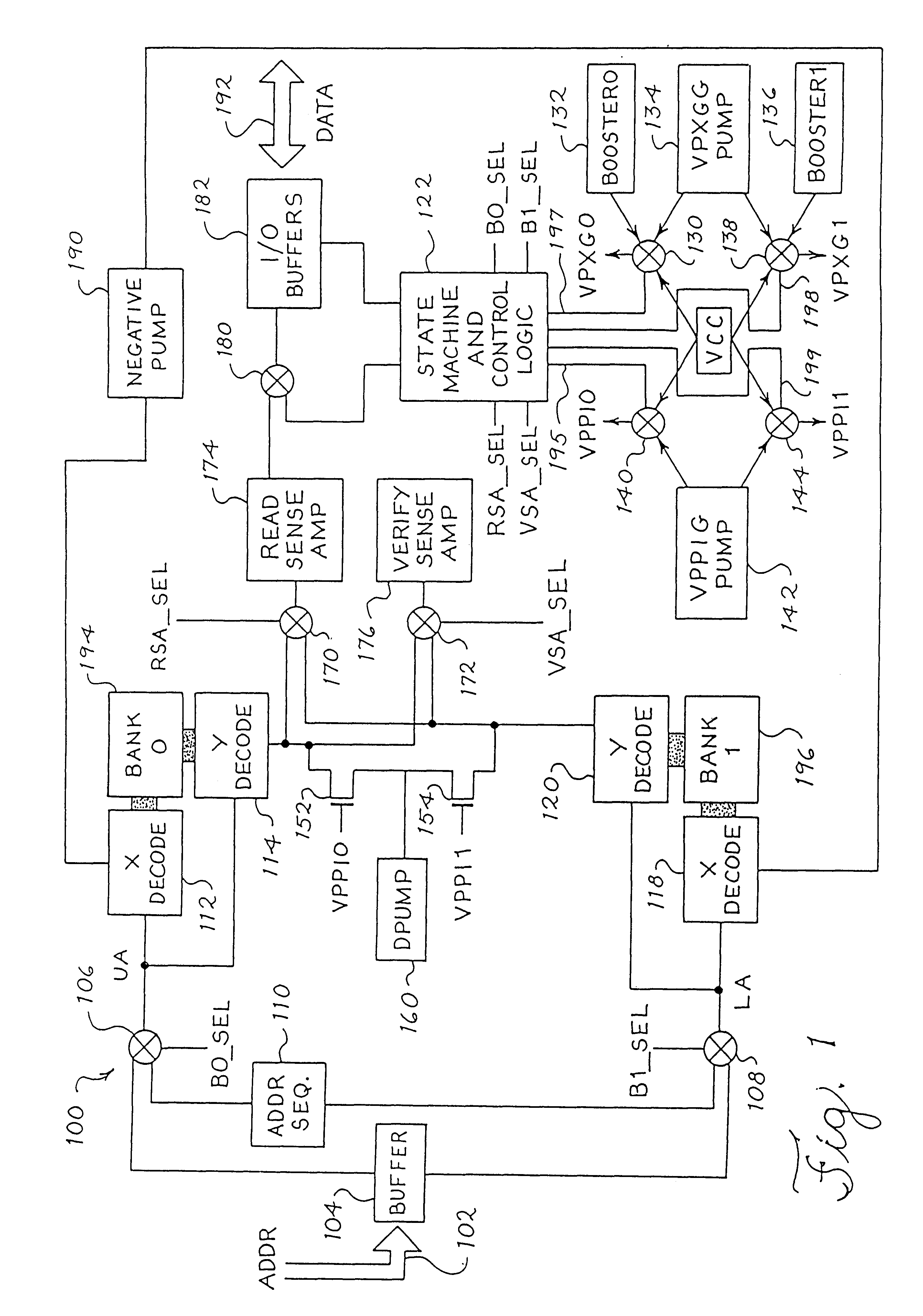
Herein, the phrase "coupled with" is defined to mean directly connected to or indirectly connected with through one or more intermediate components. Referring now to the Figures and in particular, FIG. 1, there is schematically shown a flash memory device 100 according to the present invention that provides for reading while simultaneously undergoing a program or erase operation. The memory device 100 according to the present invention may include one or more components of the memory devices disclosed in U.S. Pat. No. 5,867,430 entitled "BANK ARCHITECTURE FOR A NON-VOLATILE MEMORY ENABLING SIMULTANEOUS READING AND WRITING," to Chen et al and U.S. Pat. No. 5,847,998 entitled "NON-VOLATILE MEMORY ARRAY THAT ENABLES SIMULTANEOUS READ AND WRITE OPERATIONS," to Van Buskirk, both of which are herein incorporated by reference and further describe the implementation and operation of a device of this type. The memory device 100 may also include one or more components of such exemplary flash ...


PUM


Abstract

A flash memory device (100) provides for simultaneous read and write operations in two banks (194, 196) of flash memory cells. A plurality of output circuits (182) switch large amounts of current during reading of stored data. To reduce noise in read circuitry (174) and write circuitry (142), a separate power supply bus (204) and ground bus (208) is provided for the output circuits. The power supply bus is independent of the power supply bus which serves the internal circuitry, such as the read circuitry and the write circuitry.

Description

COPYRIGHT NOTICEA portion of the disclosure of this patent document contains material which is subject to copyright protection. The copyright owner has no objection to the facsimile reproduction by anyone of the patent document or the patent disclosure, as it appears in the Patent and Trademark Office patent file or records, but otherwise reserves all copyright rights whatsoever.Computers, personal digital assistants, cellular telephones and other electronic systems and devices typically include processors and memory. The memory is used to store instructions (typically in the form of computer programs) to be executed and / or data to be operated on by the processors to achieve the functionality of the device. In some applications, the systems and devices may require that the instructions and / or data be retained in some form of a permanent / non-volatile storage medium so that the information is not lost when the device is turned off or power is removed. Exemplary applications include co...

Claims


Application Information

Patent Timeline
IPC IPC(8): G11C8/12G11C8/00G11C16/06G11C16/30
CPCG11C8/12G11C16/30
Inventor CHEN, JOHNNY CHUNG-LEE
Owner III HLDG 4
Learn More