
Metal oxide semiconductor capacitor utilizing dummy lithographic patterns

a technology lithographic patterns, applied in the field of metal oxide semiconductor capacitors, can solve the problems of wasting significant area by a dummy pattern, requiring a large amount of chip area, and becoming more difficult to allocate sufficient area for such capacitors

Inactive Publication Date: 2000-12-05
IBM CORP
View PDF10 Cites 24 Cited by
  • Summary
  • Abstract
  • Description
  • Claims
  • Application Information

AI Technical Summary

Problems solved by technology

However, such capacitors require a large amount of chip area.
As the density of circuits increase, it becomes more difficult to allocate sufficient area for such capacitors.
For large arrays the area wasted by a the dummy patterns can be significant.

Method used


Image

  • Metal oxide semiconductor capacitor utilizing dummy lithographic patterns
  • Metal oxide semiconductor capacitor utilizing dummy lithographic patterns
  • Metal oxide semiconductor capacitor utilizing dummy lithographic patterns

Examples


Embodiment Construction

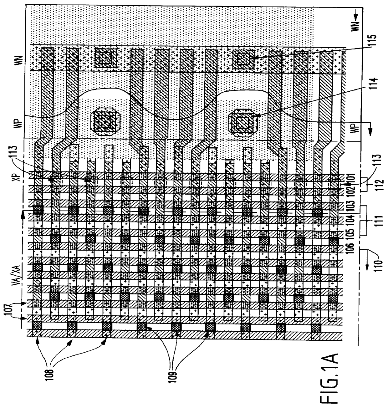
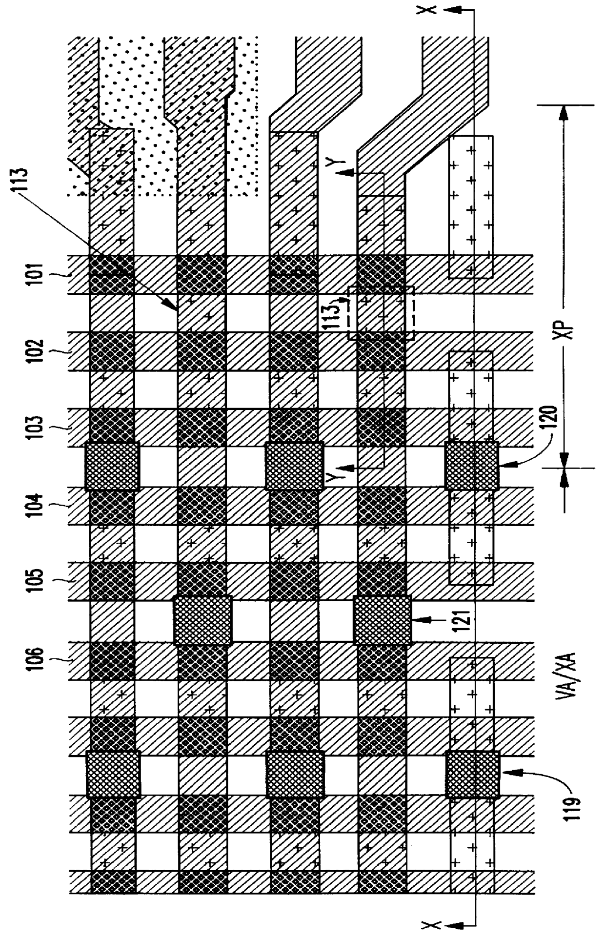
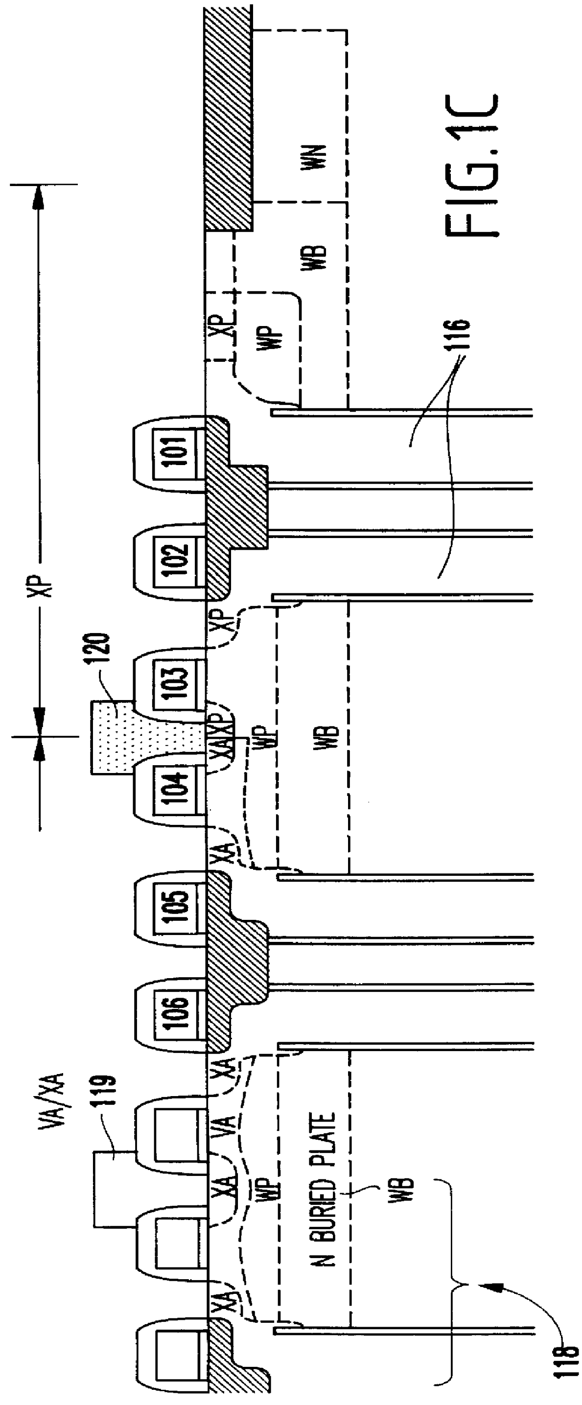
As mentioned above, it is common to form dummy patterns around the edge of a semiconductor chip array to avoid problems associated with the non-uniform patterns which form along the edges of an array. Conventional structures leave the dummy patterns unused. The invention takes advantage of these unused portions of the chip by creating passive devices such as capacitors, resistors, diodes, inductors, etc. in the unused dummy patterns

In the following discussion a large capacitor, such a decoupling capacitor, reservoir capacitor or other similar capacitor is used to illustrate features of the invention. However, the invention is not limited to a capacitor but it is equally applicable to any device which can be manufactured using the area occupied by the dummy patterns.

The usefulness of a reservoir capacitor, for example, is illustrated in the following discussion. In high density DRAM designs, a boosted wordline voltage is usually generated internally by a charge pump and then regulate...


PUM


Abstract

A semiconductor structure (and method for manufacturing the same) comprises an active array of first elements having a first manufacturing precision, a peripheral region surrounding the active array, the peripheral region including second elements having a second manufacturing precision less than the first manufacturing precision, wherein the second elements are isolated from the active array and comprise passive devices for improving operations of the active array.

Description

1. Field of the InventionThe present invention generally relates to the formation of capacitors in dynamic random access memory (DRAM) arrays and more specifically to the utilization of unused "Dummy" border areas of the DRAM arrays as capacitors and other useful structures.2. Description of the Related ArtLarge capacitors are often needed in very large scale integration (VLSI) circuits. However, such capacitors require a large amount of chip area. As the density of circuits increase, it becomes more difficult to allocate sufficient area for such capacitors.VLSI circuits, such as dynamic random access memory (DRAM) arrays have uniform repeatable shape patterns which are formed by lithographic techniques. However, due to different pattern densities, the patterns along the edges of the array are slightly different than the patterns not located along the edge (e.g., the "edge" effect). For example, elements such as via contacts that are located near the edge of the array often have pat...

Claims


Application Information

Patent Timeline
IPC IPC(8): H01L21/02H01L21/334H01L29/66H01L29/94H01L27/108H01L21/8242H01L21/70
CPCH01L29/94H01L29/66181H01L27/10897H01L27/10894H10B12/09H10B12/50H10B12/00
Inventor HSU, LOUIS L.NETIS, DMITRY
Owner IBM CORP
Learn More