
Process and device for the wave or vapor-phase soldering of electronic units

a technology of electronic components and wave or vapor phase, which is applied in the direction of electrical equipment, printed circuit manufacturing, basic electric elements, etc., can solve the problems of limited soldering temperature or soldering material, selective heating is not possible, and it is not possible with reasonable effort to solder through-hole mounting components. , to achieve the effect of high-quality solder connection

Inactive Publication Date: 2000-09-12
IBL LOTTECHN
View PDF20 Cites 16 Cited by
  • Summary
  • Abstract
  • Description
  • Claims
  • Application Information

AI Technical Summary

Benefits of technology

Building upon the state of the art referred to supra, it is an object of the present invention to provide an improved method and apparatus for soldering electronic components so that aside from lead-containing solder materials lead-free solder materials may also be used and that, moreover, conventional standard component modules may be soldered which usually are provided with components, e.g. surface mount devices, to be soldered and with components the contact legs of which protrude through the component support and that, furthermore, heat sensitive components, e.g. electrolytic capacitors, are not damaged or destroyed by soldering, and that mass production of high quality solder connections may be realized.
The transport and / or positioning arrangement for an electronic module permits transporting and placing of the module at a predetermined exactness and stability. Also, the level of the vapor ceiling may be set and controlled with a precision depending upon the structure of the embodiment of the invention. By means of the invention, either with either measure by itself or in combination, the heat sensitive components will be placed no more than partially within the saturated primary liquid vapor. This results in the advantage of utilizing that one of the mentioned measures for precision controlling which offers greater precision and / or higher stability. If, for instance, the level of the vapor ceiling is lowered after the soldering operation and at the same time the module is maintained in its position, a substantially vibration-free cooling of the liquid solder may be accomplished, at least during this phase.

Problems solved by technology

Its disadvantage is that aside from SMD components (more particularly tantalum capacitors) it does not also possible with reasonable effort to solder through-hole mounting components.
Moreover, selective heating is not possible, i.e. the individual components must all be temperature resistant up to the soldering temperature, which either limits the soldering temperature or the solder material, or requires retrofitting of those components which are not temperature resistant.
This affects particularly electrolytic capacitors which as a rule are designed for operating temperatures up to about 100.degree. C., but which outgas at higher temperatures, and are destroyed.
A further disadvantage is the fact that soldering temperatures have to be chosen which lie about 50.degree. C. above the melting temperature, for instance 183.degree. C. in the case of eutectic lead-tin solder in order to yield the best possible wetting and spreading of the solder.
The disadvantage of conventional wave soldering processes is that they usually operate in ambient atmosphere so that upon separation of the solder wave from the lower surface of the component support, bridges and burrs will form which permit soldering at spacings of up to about 0.5 mm only.
Further limitations result from the use of lead-free solders the melting temperatures of which lie significantly above the melting temperatures of 183.degree. C. of eutectic lead-tin solders often used at present.
As a result of the preheating, any solder layer on the components is melting and thus affects melting of the solder.
The drawback of the invention described in German published patent specification DE-AS 2,442,180 is that temperature sensitive components have to be retrofitted because of the non-selectivity of the soldering process.
This is especially disadvantageous in mass production because it necessitates additional process steps and because selective retrofitting of individual components is involved and often cannot be performed with the necessary quality.

Method used


Image

  • Process and device for the wave or vapor-phase soldering of electronic units
  • Process and device for the wave or vapor-phase soldering of electronic units
  • Process and device for the wave or vapor-phase soldering of electronic units

Examples


first embodiment

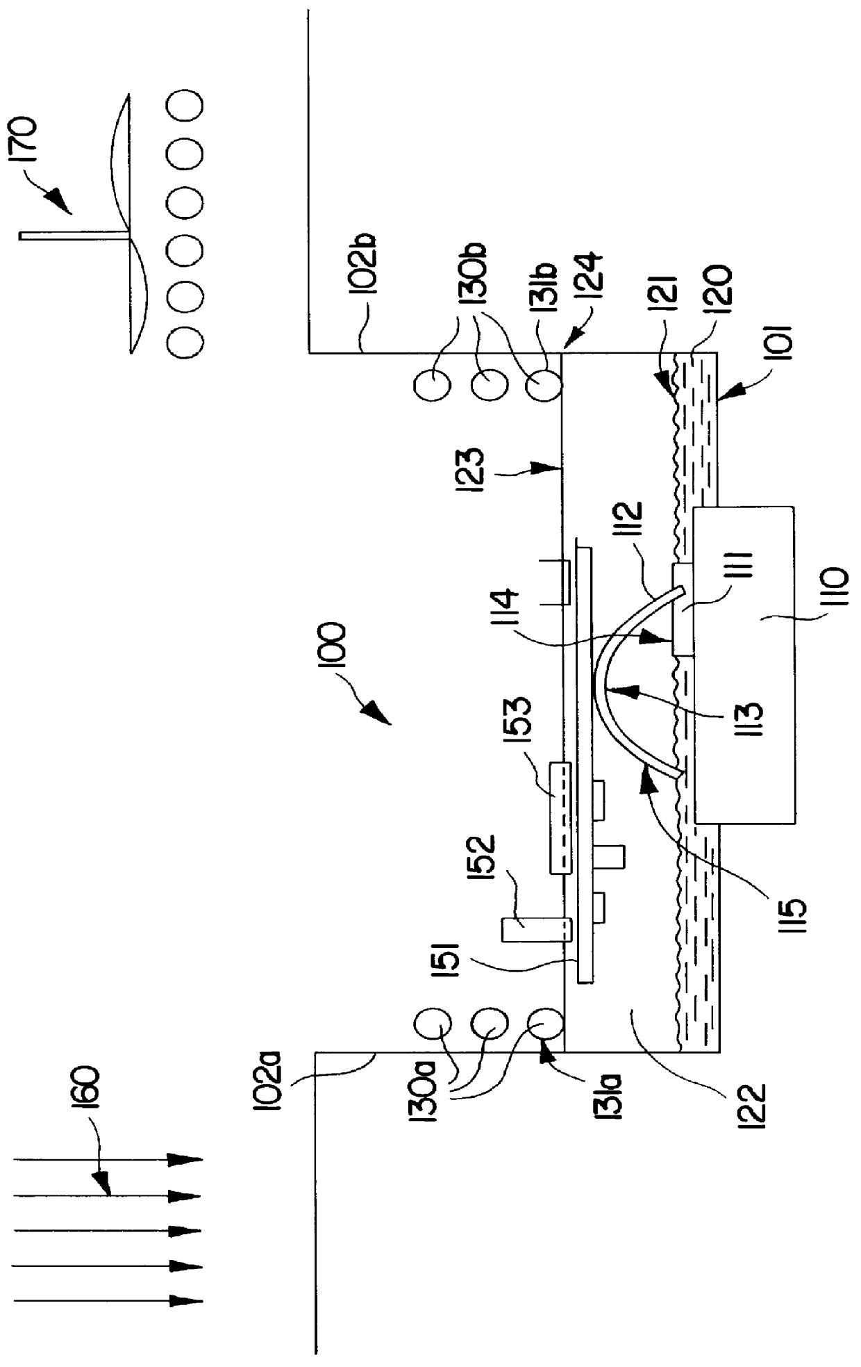
an apparatus in accordance with the invention is shown in FIG. 1. In FIG. 1, there is schematically shown a soldering chamber (100) with a portion of a solder wave module (110) penetrating into it. The lower portion of the space of the soldering chamber serves as a primary liquid reservoir, the primary liquid (120) covering the bottom (101) of the chamber and extending up to a predetermined height of the chamber. By a heating arrangement not shown in FIG. 1 the primary liquid is evaporated. The saturated primary liquid vapor (122) directly fills a portion of the volume of the chamber above the surface (121) of the primary liquid. In an upward direction the primary liquid vapor is limited by its vapor ceiling (123), the level of the vapor ceiling being set to a desired value by cooling arrangements (130a), (130b) mounted at the side walls (102a), (102b) of the chamber.

The cooling arrangements (130a), (130b) may be submerged into, and withdrawn from, the vapor in a direction parallel ...


PUM

PropertyMeasurementUnit
Angleaaaaaaaaaa
Temperatureaaaaaaaaaa
Sizeaaaaaaaaaa

Abstract

PCT No. PCT / DE96 / 00968 Sec. 371 Date Dec. 12, 1997 Sec. 102(e) Date Dec. 12, 1997 PCT Filed May 24, 1996 PCT Pub. No. WO96 / 37330 PCT Pub. Date Nov. 28, 1996A method of and an apparatus for vapor phase / solder wave soldering contacts of electronic components including temperature sensitive portions in which the components while moving through a soldering chamber are only partially immersed in a saturated vapor whereas the contacts are wholly immersed in the vapor. A solder wave having a crest substantially coinciding with the components to be soldered is provided within the saturated vapor and a layer of an inert gas is provided above the vapor ceiling.

Description

1. Field of the InventionThe invention relates to a method and an apparatus for wave and / or vapor phase soldering of electronic components.The invention may be used in the fabrication of electronic components in which soldering has nowadays to be performed in through-hole mounting on conventional components as well as on surface mount devices (SMD). Another field of application of the invention is soft-soldering of metallic semi-fabricated components.2. State of the ArtIt is well known that for soldering surface mount devices, reflow soldering processes are used. In such processes, the desired solder connections are fabricated by solder being reflowed and remelted as a solder paste by the application of energy. In known reflow soldering processes infrared radiation (infrared soldering) or hot gas (convection soldering), more particularly nitrogen, or laser radiation (laser soldering) or saturated vapor as in vapor phase soldering, are used. The most common processes utilized nowaday...

Claims


Application Information

Patent Timeline
IPC IPC(8): B23K1/015B23K1/012H05K3/34B23K1/08
CPCB23K1/015H05K3/3494B23K2201/40H05K3/3415H05K3/3468H05K2203/088B23K2101/40
Inventor SCHEEL, WOLFGANGRING, KARLHAFNER, WILLILEICHT, HELMUT
Owner IBL LOTTECHN
Learn More