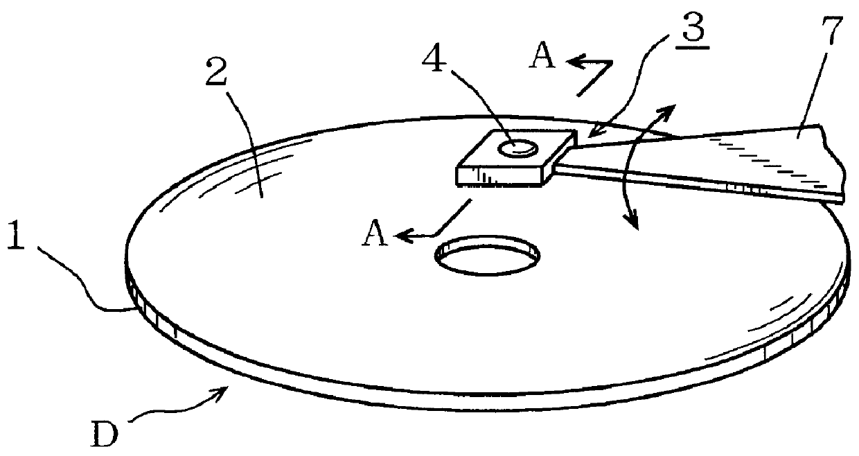
Optical system for optical recording
an optical recording and optical head technology, applied in the field of optical recording systems, can solve the problems of striae, optical head with excellent performance cannot be provided, and the conventional glasses have had problems such as stria
- Summary
- Abstract
- Description
- Claims
- Application Information
AI Technical Summary
Benefits of technology
Problems solved by technology
Method used
Image
Examples
embodiment 1
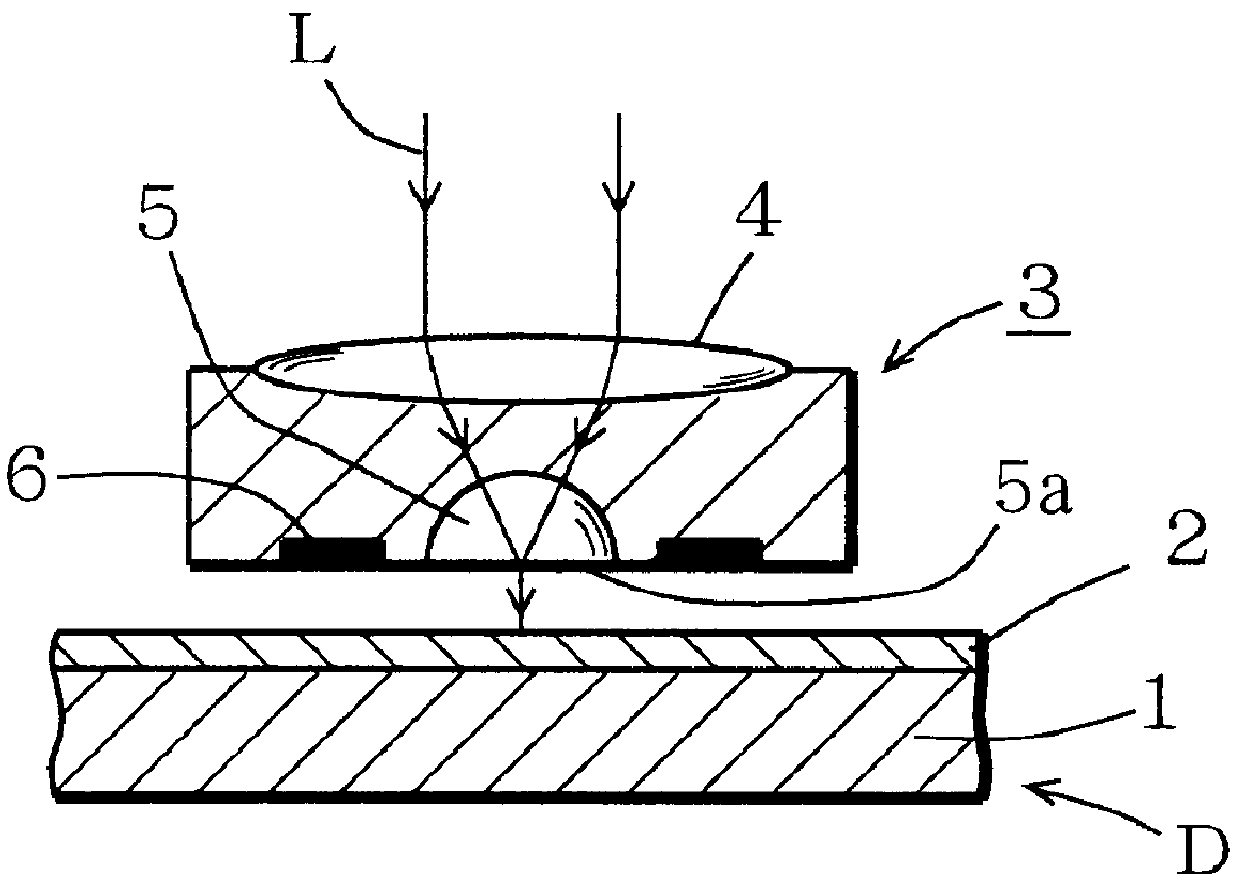
Two substrates of 3 inch in diameter and 1 mm in thickness were cut out with a fixed orientation from a 3-inch LiTaO3 single crystal produced by Czochralski method. Both faces were optically-polished and the substrates were bonded together with a wax of low viscosity. Next, a 2 mm cube was cut out of the substrates, and a spherical lens of 1 mm in diameter was produced by the conventional polishing process of a n optical ball lens. Next, this spherical lens was immersed in a wax removing solution and rinsed to produce hemispheric lenses of 1 mm in diameter.
As these hemispheric lenses were produced by the production process of optical ball lens, the working accuracy was equal to that of the spherical lens. The direction of the incident laser beam was controlled within 0.1 degree from the optic axis so as to minimize the effects of double refraction. As a result, a condenser lens mainly for ordinary ray was produced. An outgoing ray of a semiconductor laser of 635 nm in wavelength is ...
embodiment 2
A single crystal of rutile phase TiO2 of about 2 inches in diameter was obtained by Czochralski method using a crystal growth furnace of resistance heating process. Substrates of 1 mm in thickness were cut with a fixed orientation along with the face c from the above-mentioned single crystal of rutile phase TiO2 so that the optic axis (Z axis (c axis)) was perpendicular to the recording side of an optical magnetic disc (the refractive index is 2.61 because the refractive index for ordinary ray and the refractive index for extraordinary ray are identical to each other). Both faces of these substrates were polished and the substrates were bonded together with a wax of low viscosity. Next, the cubes of which one side is 2 mm were cut out of the bonded substrates, and spherical lenses of 1 mm in diameter were produced by a conventional polishing process for optical ball lens. Then these spherical lenses were immersed in a wax removing solution and rinsed to obtain hemispheric lenses of ...
embodiment 3
In a way similar to the embodiment 2, a single crystal of LiNbO3 of about 3 inches in diameter was obtained by Czochralski method using a crystal growth furnace of resistance heating process. Magnesia was added to the raw material for growing a single crystal so that the content of magnesia after crystal growth is 5 mol %.
The light-induced refractive index change of this single crystal of LiNbO3 is measured by Senarmont method. It was about 1.2.times.10.sup.-6, and the refractive index distribution was 1.times.10.sup.-4 or under and was very small in comparison with that of the above-mentioned glass. Substrates of 0.75 mm in thickness were cut with a fixed orientation along the face c from the above-mentioned single crystal of LiNbO3 so that the optic axis (Z axis (c axis)) was perpendicular to the recording side of an optical magnetic disc (the refractive index is 2.29 because the refractive index for ordinary ray and the refractive index for extraordinary ray are identical to each...
PUM
| Property | Measurement | Unit |
|---|---|---|
| refractive index | aaaaa | aaaaa |
| angle | aaaaa | aaaaa |
| angle | aaaaa | aaaaa |
Abstract
Description
Claims
Application Information
 - R&D
- Intellectual Property
- Life Sciences
- Materials
- Tech Scout
- Unparalleled Data Quality
- Higher Quality Content
- 60% Fewer Hallucinations
Browse by: Latest US Patents, China's latest patents, Technical Efficacy Thesaurus, Application Domain, Technology Topic, Popular Technical Reports.
© 2025 PatSnap. All rights reserved.Legal|Privacy policy|Modern Slavery Act Transparency Statement|Sitemap|About US| Contact US: help@patsnap.com


