
Macrocell for data processing circuit

a data processing circuit and macrocell technology, applied in the direction of logic circuits, electric digital data processing, instruments, etc., can solve the problems of limiting the reusability of macrocells, adding design costs, and discharging power

Inactive Publication Date: 2000-03-07
ARM LTD
View PDF6 Cites 9 Cited by
  • Summary
  • Abstract
  • Description
  • Claims
  • Application Information

AI Technical Summary

Benefits of technology

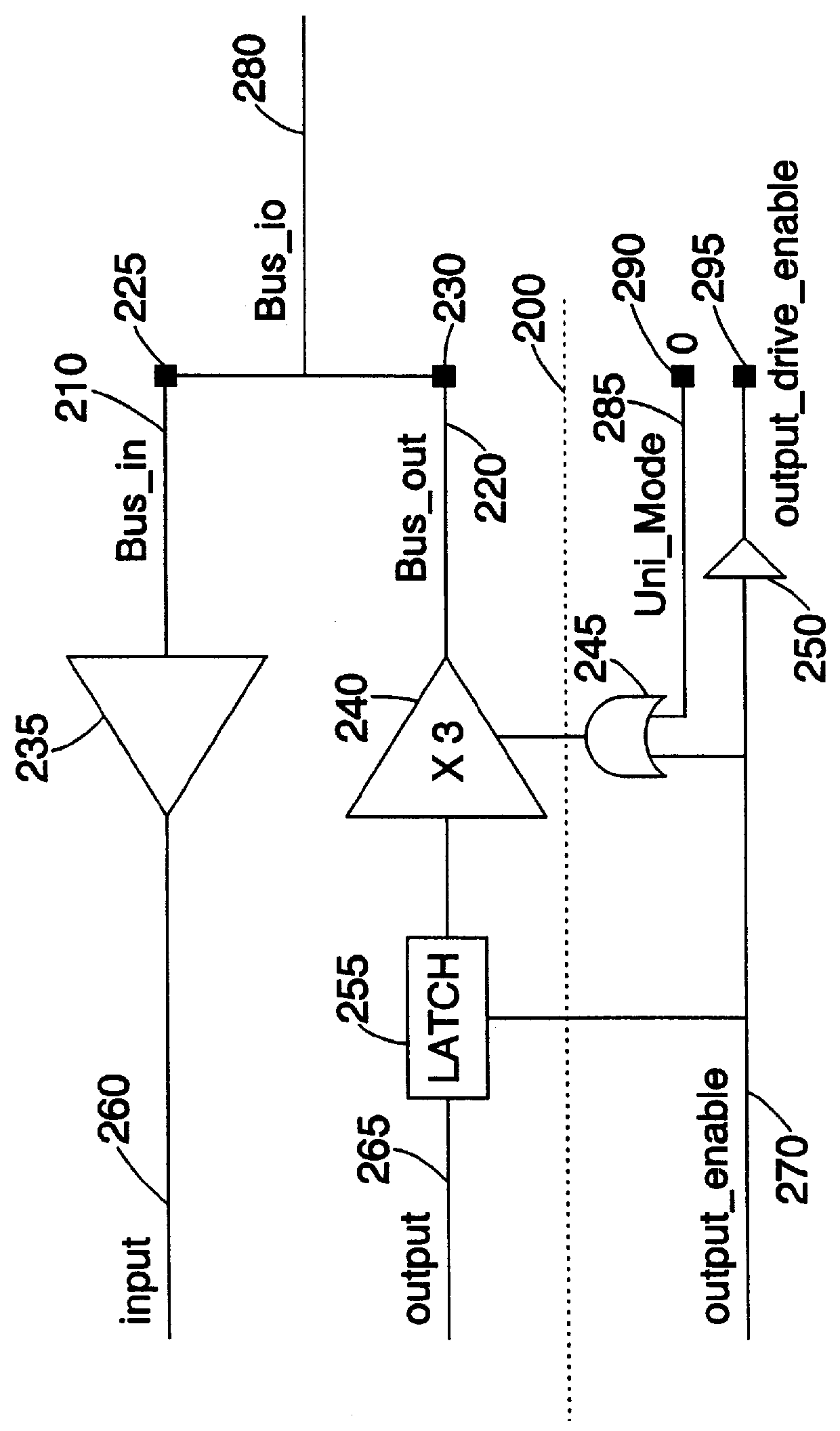
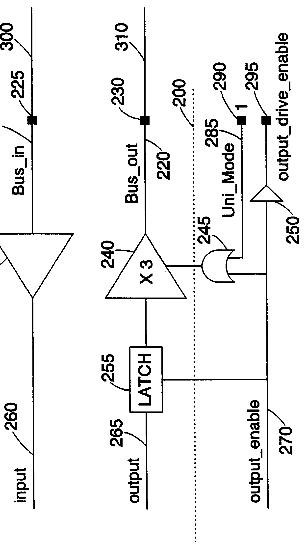
Preferably, the second mode value is a logic `1` level signal which, when the macrocell is arranged to be coupled to a unidirectional bus on the data processing circuit, causes the tristate buffer to be turned on so as to permanently drive the output bus. Further, in preferred embodiments, the first mode value is a logic `0` level signal which, when the macrocell is arranged to be coupled to a bidirectional bus on the data processing circuit, causes the tristate buffer to be turned on only when the output enable signal is at a logic `1` level, thereby causing the tristate buffer to enter a high impedance state when no data is being output from the macrocell.

Problems solved by technology

However, this adds to design cost, and limits the reusability of macrocells.
However, in preferred embodiments, only one mode input terminal will be provided for the whole macrocell, since the whole macrocell will typically be configured with all drivers unidirectional or bidirectional.
This is not desirable, since any change of the output bus values will drive any connected circuitry, thereby dissipating power.

Method used


Image

  • Macrocell for data processing circuit
  • Macrocell for data processing circuit
  • Macrocell for data processing circuit

Examples


Embodiment Construction

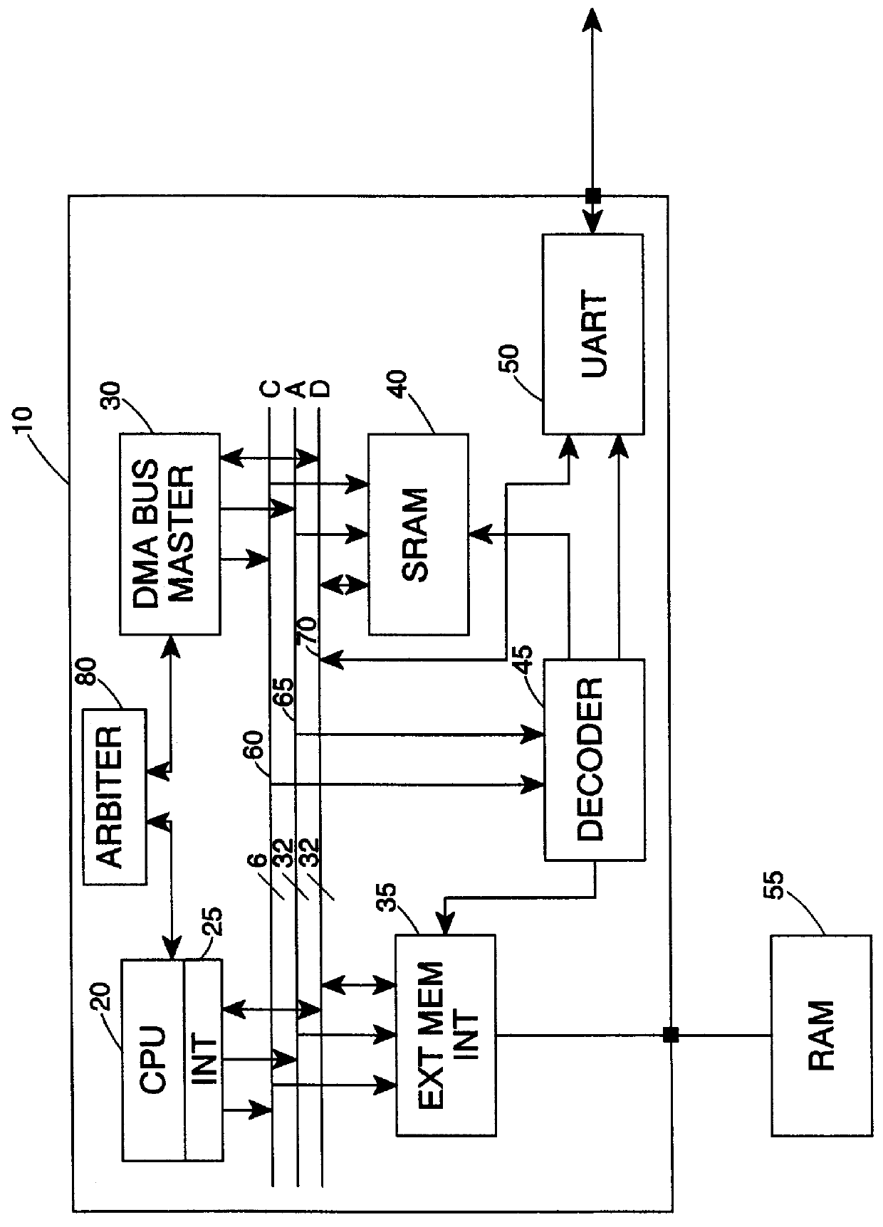
FIG. 1 is a block diagram of a data processing circuit, in this case a chip 10. which illustrates a number of macrocells that may be provided on the chip 10. along with their various connections to a number of buses provided on the chip 10.

Within the chip 10 illustrated in FIG. 1, a CPU 20 and a Direct Memory Access (DMA) bus master 30 are provided, which are able to output signals onto control 60 and address 65 buses, and also to output data onto, and receive data from, a data bus 70. Both the CPU 20 and DMA bus master 30 are referred to as "Bus Masters", since these macrocells are used to control the transfer of data over the buses.

To avoid contention between the Bus Masters, arbiter logic 80 is provided, which is arranged to select the Bus Master that is to be active on the bus at any particular time. In the present example, the arbiter 80 hence decides which of the CPU 20 or DMA bus master 30 is allowed, at any particular moment in time, to drive the address and control buses 60...


PUM


Abstract

The present invention provides a macrocell for a data processing circuit, comprising macrocell logic, and an interface for connecting the macrocell logic to a bus of the data processing circuit. The interface comprises: an input bus connected to an input bus terminal, an output bus connected to an output bus terminal, and a buffering circuit for buffering the output bus from the macrocell logic. Further, the interface has a mode input terminal for receiving a mode value, the mode value being arranged to control the buffering circuit. The buffering circuit is responsive to a first mode value to enter an inactive state when no data is being output from the macrocell, and is responsive to a second mode value to permanently drive the output bus. Hence, to enable the macrocell to be coupled to a unidirectional bus on the data processing circuit, the second mode value is supplied to the mode input terminal, whilst to enable the macrocell to be coupled to a bidirectional bus on the data processing circuit, the input bus terminal and output bus terminal are connected together externally to the macrocell, and the first mode value is supplied to the mode input terminal.

Description

1. Field of the InventionThe present invention relates to macrocells for data processing circuits. For the purpose of the present application, the term "macrocell" refers to any physically or logically modular component for a data processing circuit, for example a raw processor core, a cache, a memory management unit (MMU), or even a processor with cache and MMU, etc.2. Description of the Prior ArtTypically, a data processing circuit such as a chip will include a number of macrocells that are arranged to interact with each other to perform data processing operations. Modular components such as the central processing unit, or processor core, used to apply instructions to data items read from memory, one or more caches or memories used to store instructions and data, a DMA bus master used to control activities such as data transfer, and an external memory interface for holding data to be output from the chip to memory, are examples of components which may be formed as macrocells.Durin...

Claims


Application Information

Patent Timeline
IPC IPC(8): H03K19/173
CPCH03K19/1733
Inventor FLYNN, DAVID WALTER
Owner ARM LTD
Learn More