Defect detection device, defect detection method, and defect observation apparatus including defect detection device

Pending Publication Date: 2022-05-19
HITACHI HIGH-TECH CORP
View PDF0 Cites 0 Cited by
  • Summary
  • Abstract
  • Description
  • Claims
  • Application Information

AI Technical Summary

Benefits of technology

This patent aims to address a technical problem by introducing a new technology that improves the efficiency and accuracy of a device or system. The technology can be applied to a variety of applications and can enhance the performance of the device or system in a specific way.

Problems solved by technology

However, the defect inspection apparatus and the defect observation apparatus are separate apparatuses, and it is difficult to position a defect in a field of view of the SEM-type defect observation apparatus only based on the defect position information calculated by the defect inspection apparatus due to deviation of stage coordinates between the apparatuses, or the like.

Method used


Image

  • Defect detection device, defect detection method, and defect observation apparatus including defect detection device
  • Defect detection device, defect detection method, and defect observation apparatus including defect detection device
  • Defect detection device, defect detection method, and defect observation apparatus including defect detection device

Examples


first embodiment

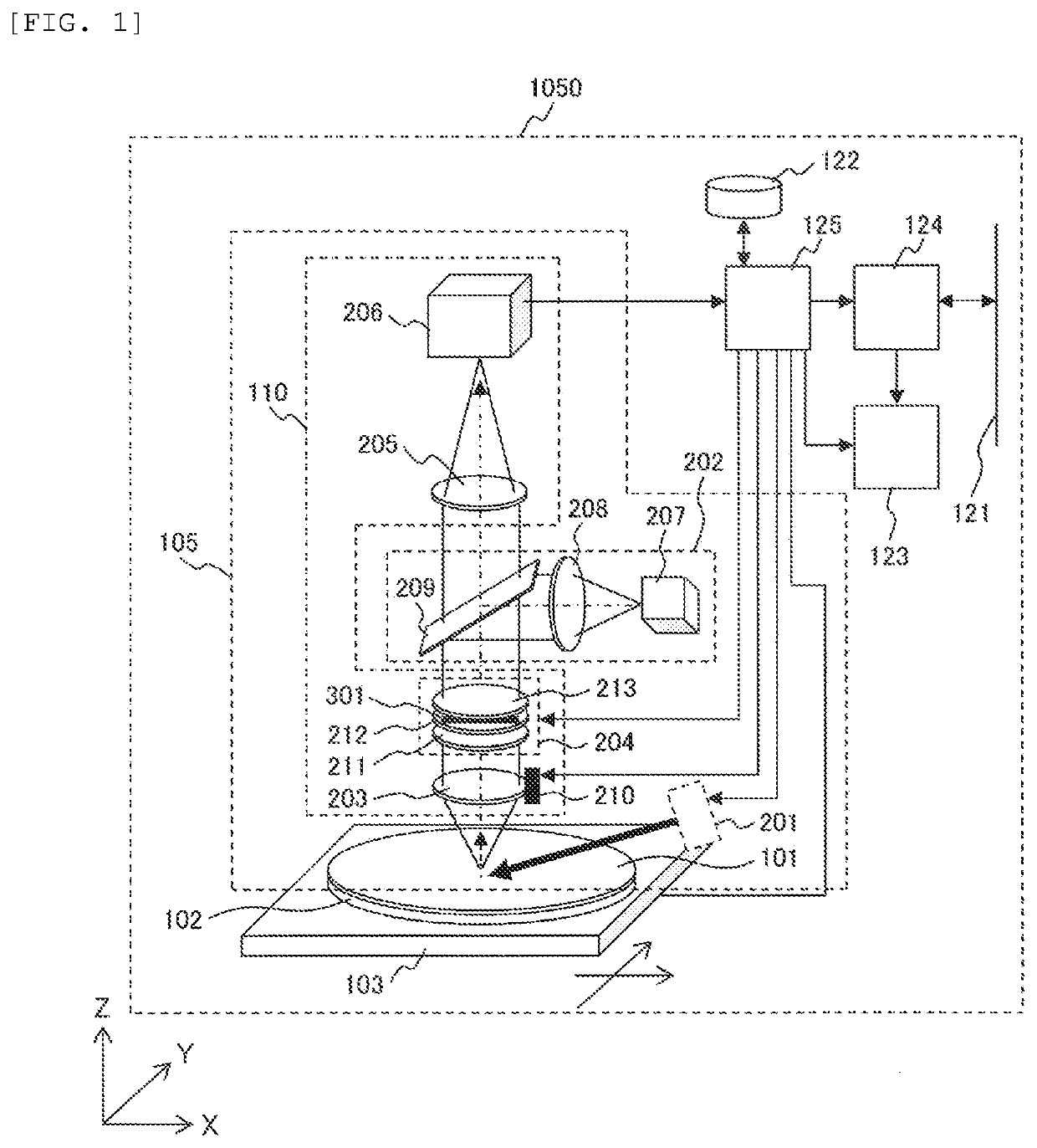
[0043]FIG. 1 shows an example of a configuration of a defect detection device according to a first embodiment of the invention. The defect detection device according to the present embodiment is a defect detection device that detects a defect on a wafer generated in a manufacturing process of a semiconductor device or a defect detection device mounted on a defect observation apparatus.

[0044]A reference numeral 1050 denotes the defect detection device. The defect detection device 1050 generally includes a sample holder 102, a stage 103, an optical microscope unit 105, a network 121, a database 122, a user interface 123, a storage device 124, and a control system unit 125.

[0045]A reference numeral 101 denotes the wafer which is a sample to be inspected. A reference numeral 102 denotes the sample holder on which the wafer 101 is placed. A reference numeral 103 denotes the stage on which the sample holder 102 can be placed, and which allows any position of the wafer 101 to be moved in a...

second embodiment

[0081]FIG. 11 shows an example of a configuration of a defect detection device 1051 according to a second embodiment of the invention. In the present embodiment, a Fourier transform plane observation system 235 that observes a Fourier transform plane 301 which is a pupil plane of the objective lens 203 is mounted, and it is possible to observe a Fourier transform plane to be observed. A basic configuration of the defect detection device 1051 is substantially the same as the configuration of the defect detection device 1050 described with reference to FIG. 1 in the first embodiment, and the same components are denoted by the same reference numerals. In order to avoid redundant description, only differences from the defect detection device 1050 described with reference to FIG. 1 will be described below.

[0082]An optical microscope unit 105-1 of the defect detection device 1051 according to the present embodiment includes the Fourier transform plane observation system 235, and is connec...

third embodiment

[0099]FIG. 14 shows an example of a configuration of a defect observation apparatus 1000 according to a third embodiment of the invention. The defect observation apparatus 1000 according to the present embodiment has a configuration using the defect detection device 1050 described according to the above-described first embodiment, and may have a configuration using the defect detection device 1051 described according to the second embodiment.

[0100]The defect observation apparatus 1000 schematically includes an observation device 100, a network 1210, a database 1220, a user interface 1230, a storage device 1240, and a control system unit 1250. The defect observation apparatus 1000 is connected to a defect inspection apparatus 107, which is another inspection apparatus, via the network 1210.

[0101]The defect inspection apparatus 107 detects a defect present on the wafer 101 and acquires defect information such as position coordinates and a size of the defect.

[0102]The defect informatio...


PUM


Abstract

A defect detection device including an illumination optical system, an image capturing optical system configured to capture an image of scattered light generated by the illumination optical system irradiating the wafer, and an image processing unit configured to process a picture of the image of the scattered light to extract a defect on the wafer. The image capturing optical system includes an objective lens, a filter unit configured to shield a part of light transmitted through the objective lens, and an imaging lens configured to form an image of light transmitted through the filter unit. The filter unit includes a first microlens array configured to condense parallel light transmitted through the objective lens, a shutter array including a light transmission unit at a focus position of the first microlens array, and a second microlens array disposed opposite to the first microlens array with respect to the shutter array.

Description

TECHNICAL FIELD[0001]The present invention relates to a defect detection device and a defect detection method for detecting a defect or the like generated on a semiconductor wafer in a manufacturing process of a semiconductor device, and a defect observation apparatus including the defect detection device.BACKGROUND ART[0002]Defect inspection of a foreign object defect, a pattern defect, or the like on a semiconductor wafer in a semiconductor manufacturing process is performed by defect detection and defect position calculation by a defect inspection apparatus and defect observation by a defect observation apparatus, and a process to be taken as a countermeasure is narrowed down based on an observation result of the defect. Since miniaturization of a semiconductor pattern progresses and a fine defect also affects a yield, a scanning electron microscope (SEM) is used for the observation apparatus.[0003]The defect inspection apparatus and the SEM-type defect observation apparatus are ...

Claims


Application Information

Patent Timeline
IPC IPC(8): G01N21/95G01N21/88G02B5/20G02B3/00
CPCG01N21/9501G01N21/8806G02B3/0006G02B5/20G01N21/8851G01N21/95623H01L22/12G02B21/0016G02B21/361G02B21/365G02B21/14G01N21/956G01N2201/0639G01N2201/0648
Inventor OTANI, YUKOAOKI, KAZUOMATSUMOTO, SHUNICHIURANO, YUTA
Owner HITACHI HIGH-TECH CORP
Why Eureka
Try Eureka