Radio-frequency signal transmitting/receiving circuit

Pending Publication Date: 2022-05-12
MURATA MFG CO LTD
View PDF0 Cites 0 Cited by
  • Summary
  • Abstract
  • Description
  • Claims
  • Application Information

AI Technical Summary

Benefits of technology

The patent aims to prevent a RF transmission signal from interfering with multiple reception paths. The technical effect is to enhance the quality of RF signal transmission.

Problems solved by technology

However, with the semiconductor device described in JP-A No. 2003-179521, a transmission signal mixed in multiple reception paths may not be suppressed.

Method used


Image

  • Radio-frequency signal transmitting/receiving circuit
  • Radio-frequency signal transmitting/receiving circuit
  • Radio-frequency signal transmitting/receiving circuit

Examples


first embodiment

Circuit Configuration

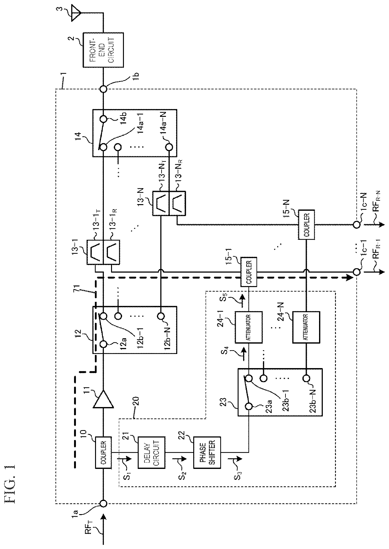
[0020]FIG. 1 is a diagram illustrating the configuration of an RF signal transmitting / receiving circuit according to the first embodiment. An RF signal transmitting / receiving circuit 1 is an RF signal transmitting / receiving module capable of outputting an RF transmission signal RFT via a front-end circuit 2 to an antenna 3 and receiving RF reception signals RFR-1 to RFR-N via the front-end circuit 2 from the antenna 3 in a mobile communication apparatus exemplified by a cellular phone. The RF signal transmitting / receiving module may be configured by mounting one or more components on a substrate.

[0021]The frequencies of the RF transmission signal RFT and the RF reception signals RFR-1 to RFR-N are exemplified by about several hundred megahertz (MHz) to several tens of gigahertz (GHz), but the present disclosure is not limited to these frequencies.

[0022]The RF signal transmitting / receiving circuit 1 performs frequency division duplex (FDD).

[0023]The RF signal tra...

specific examples

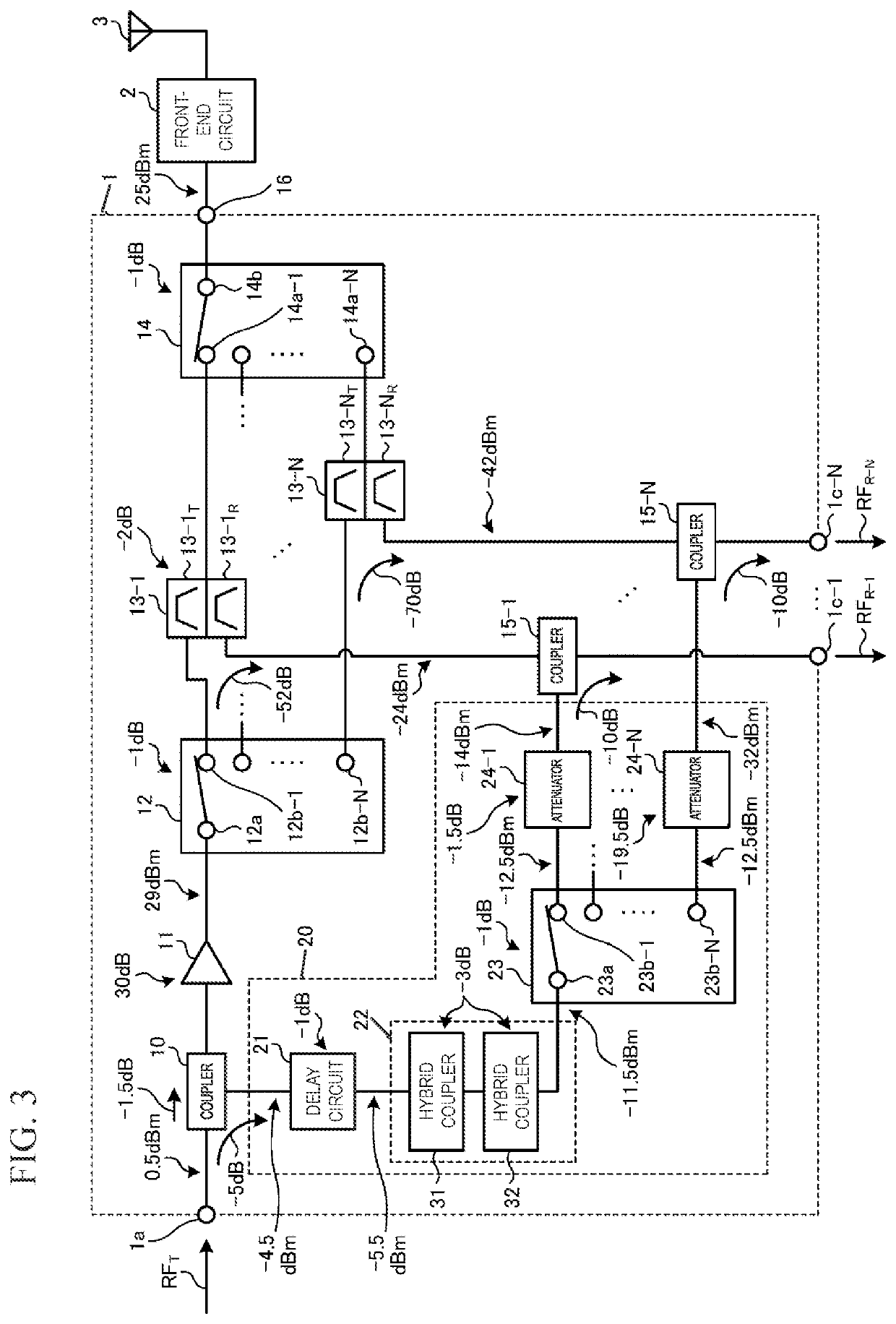
[0074]FIG. 3 is a diagram illustrating a specific example of the loss and gain, and signal power of each part of the RF signal transmitting / receiving circuit according to the first embodiment.

first case

[0075]The power of the RF transmission signal RFT input to the coupler 10 is about 0.5 dBm. The loss of the coupler 10 is about −1.5 dB to the power amplifier circuit 11 side and is about −5 dB to the delay circuit 21 side.

[0076]The power of the RF transmission signal RFT input from the coupler 10 to the power amplifier circuit 11 is approximately −1 dBm (=0.5−1.5). The gain of the power amplifier circuit 11 is about 30 dB. The power of the RF transmission signal RFT output from the power amplifier circuit 11 is approximately 29 dBm (=−1+30).

[0077]The loss of the switch 12 is approximately −1 dB. The loss of the transmission filter 13-1T is approximately −2 dB. The loss of the switch 14 is approximately −1 dB. Therefore, the power of the RF transmission signal RFT output from the input / output terminal 1b to the front-end circuit 2 is about 25 dBm (=29−1−2−1).

[0078]The loss due to isolation between the transmission filter 13-1T and the reception filter 13-1R of the duplexer 13-1 is a...


PUM


Abstract

An RF signal transmitting / receiving circuit includes: at least one power amplifier circuit that amplifies and outputs an RF transmission signal; duplexers each including a transmission filter that passes the RF transmission signal amplified by the power amplifier circuit, and a reception filter that passes an RF reception signal; at least one distribution circuit that divides the RF transmission signal input to the power amplifier circuit and outputs a first signal; a signal output circuit that outputs, based on the first signal, in at least one transmission path among transmission paths of a plurality of the RF reception signals, at least one second signal that has substantially a same delay amount, an inverted phase, and substantially same power as the RF transmission signal mixed in the RF reception signal; and coupling circuits that couple the second signal to the RF reception signal transmitted in the at least one transmission path.

Description

CROSS REFERENCE TO RELATED APPLICATION[0001]This application claims priority from Japanese Patent Application No. 2020-186703 filed on Nov. 9, 2020. The content of this application is incorporated herein by reference in its entirety.BACKGROUND[0002]The present disclosure relates to a radio-frequency (RF) signal transmitting / receiving circuit.[0003]Japanese Unexamined Patent Application Publication (JP-A) No. 2003-179521 describes a semiconductor device that cancels out a leakage signal from a high power amplifier to a reception channel. Other related technology is described in, for example, JP-A Nos. 2011-120120 and H11-308143.[0004]Recently, an RF signal transmitting / receiving circuit includes multiple reception paths for performing reception in multiple bands. However, with the semiconductor device described in JP-A No. 2003-179521, a transmission signal mixed in multiple reception paths may not be suppressed.BRIEF SUMMARY[0005]The present disclosure suppresses an RF transmission ...

Claims


Application Information

Patent Timeline
IPC IPC(8): H04B1/40H04L5/14
CPCH04B1/40H04L5/14
Inventor TAKEZONO, NAOFUMI
Owner MURATA MFG CO LTD
Why Eureka
Try Eureka