Antenna structure and electronic device including same

an antenna device and electronic device technology, applied in the field of antenna device structure and electronic device, can solve the problems of reducing affecting the operation affecting the performance of the antenna device, so as to ensure the radiation performance, reduce signal interference, and secure stable radiation performance

Pending Publication Date: 2022-04-28
SAMSUNG ELECTRONICS CO LTD +1
View PDF0 Cites 2 Cited by
  • Summary
  • Abstract
  • Description
  • Claims
  • Application Information

AI Technical Summary

Benefits of technology

The patent describes an antenna structure and electronic device that can provide stable wireless communication by reducing interference from the environment. The antenna structure includes a housing with at least one slot that acts as an antenna for millimeter wave communication. The slot is connected to a communication circuit, which radiates an antenna beam to reduce signal interference and ensure good radiation performance. The electronic device can also include a phased array antenna for transmitting and receiving millimeter waves. Additionally, the antenna structure has multiple feeding units that can independently apply signals, making it easy to adjust the resonant frequency.

Problems solved by technology

Since the resonant frequency wavelength of the antenna device used for 5G communication (or mmWave communication) merely ranges from about 1 mm to about 10 mm, the radiation performance of the antenna device may be significantly distorted depending on the installation environment due to its high straightness and directivity.
For example, when an antenna device for mmWave communication is equipped in an electronic device, the performance of the antenna device may be lowered due to interference by the structures around the electronic device or the user's body.
Further, it may be difficult to exhibit the optimized operating characteristics of the antenna device because the bezel design of the material of the electronic device, e.g., a metal material, is not considered.
Further, slot-type antenna devices known so far may form a single slot antenna structure, which may not easily support a wider frequency band.

Method used


Image

  • Antenna structure and electronic device including same
  • Antenna structure and electronic device including same
  • Antenna structure and electronic device including same

Examples


Embodiment Construction

[0057]FIGS. 1 through 19C, discussed below, and the various embodiments used to describe the principles of the present disclosure in this patent document are by way of illustration only and should not be construed in any way to limit the scope of the disclosure. Those skilled in the art will understand that the principles of the present disclosure may be implemented in any suitably arranged system or device.

[0058]Hereinafter, embodiments of the present disclosure are described with reference to the accompanying drawings.

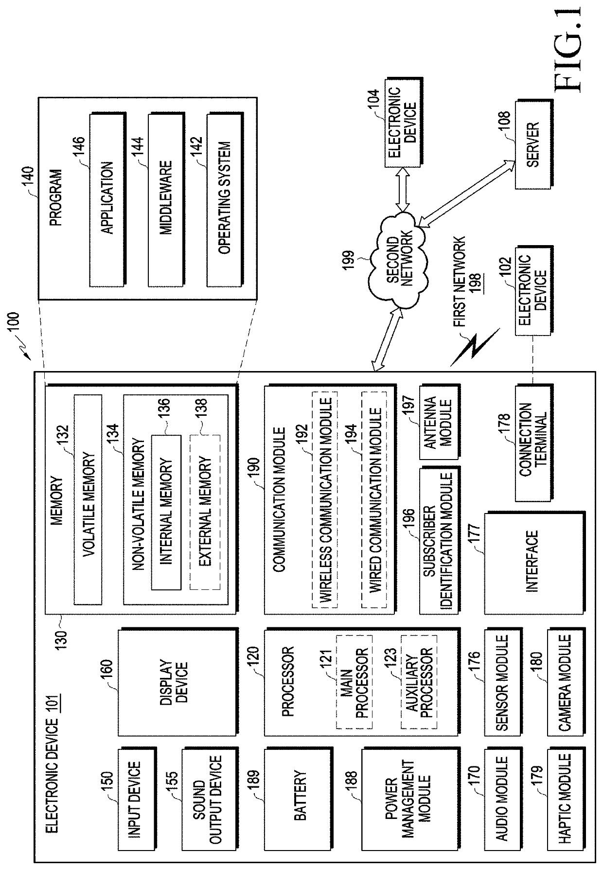
[0059]FIG. 1 is a block diagram illustrating an electronic device 101 in a network environment 100 according to various embodiments.

[0060]Referring to FIG. 1, the electronic device 101 in the network environment 100 may communicate with an electronic device 102 via a first network 198 (e.g., a short-range wireless communication network), or an electronic device 104 or a server 108 via a second network 199 (e.g., a long-range wireless communication network). According...


PUM


Abstract

Electronic device is provided. The electronic device comprises: a housing surrounding a space between first and second plates and including a side surface member of which at least a portion includes a conductive section; a communication module; and an antenna structure. The conductive section includes first and second regions formed at a different position. The antenna structure includes a plurality of first slot sets formed in the first region, wherein at least two first slots extending in a first direction combine to form one first slot set and the plurality of first slot sets are formed at first designated intervals in a second direction, and a plurality of second slot sets formed in the second region. At least two second slots extending in the first direction combine to form one second slot set and the plurality of second slot sets are formed at second designated intervals in the second direction.

Description

CROSS-REFERENCE TO RELATED APPLICATIONS[0001]This application is a Bypass Continuation of International Application No. PCT / KR2020 / 008748, filed Jul. 3, 2020, which claims priority to Korean Patent Application No KR 10-2019-0081649, filed Jul. 5, 2019, the disclosures of which are herein incorporated by reference in their entirety.BACKGROUND1. Field[0002]Various embodiments of the disclosure relate to an antenna structure providing a wireless communication function and an electronic device including the same.2. Description of Related Art[0003]The provision of services of constant quality over a commercially available wireless communication network need meet a high antenna device gain and a broad beam coverage area. A next-generation mobile communication service (e.g., 5G communication) with a frequency band of a few tens of GHz (e.g., a frequency band ranging from 30 GHz to 300 GHz and a resonant frequency wavelength ranging about 1 mm to about 10 mm) implements easy connection (e.g...

Claims


Application Information

Patent Timeline
Patent Type & Authority Applications(United States)
IPC IPC(8): H01Q21/06H04M1/02
CPCH01Q21/064H01Q1/243H04M1/0266H04M1/0214H04M1/026H01Q21/28H01Q3/242H01Q21/30H01Q1/38H04M1/0249H04M1/0277H04M1/0216H01Q1/46H01Q21/06
Inventor KIM, JUNGGILYOON, YOUNGJOONGKIM, SUNGSOOKIM, SUNGHOEBAE, JANGHWAN
Owner SAMSUNG ELECTRONICS CO LTD
Why Eureka
Try Eureka