Organic Compound, Light-Emitting Device, Light-Emitting Apparatus, Electronic Device, Display Device, and Lighting Device
- Summary
- Abstract
- Description
- Claims
- Application Information
AI Technical Summary
Benefits of technology
Problems solved by technology
Method used
Image

Examples
embodiment 1
[0077]In this embodiment, an organic compound of one embodiment of the present invention will be described.
EXAMPLE 1 OF ORGANIC COMPOUND
[0078]The organic compound described in this embodiment is an organic compound represented by General Formula (G1) below.
[Chemical Formula 4]
E-Ar-A (G1)
EXAMPLE OF E
[0079]In General Formula (G1) above, E represents a substituted or unsubstituted naphtho[2,3-c]carbazolyl group or a substituted or unsubstituted benzo[c]naphtho[2,3-g]carbazolyl group. Note that as a substituent, an aryl group having 6 to 13, inclusive, carbon atoms, an alkyl group having 1 to 6, inclusive, carbon atoms, or a cycloalkyl group having 6 to 10, inclusive, carbon atoms can be used. For example, a phenyl group, a biphenyl group, a naphthyl group, or a fluorenyl group can be used as the substituent. The aryl group may include one or two alkyl groups each having 1 to 6, inclusive, carbon atoms or one or two cycloalkyl groups each having 6 to 10, inclusive, carbon atoms. Alter...
embodiment 2
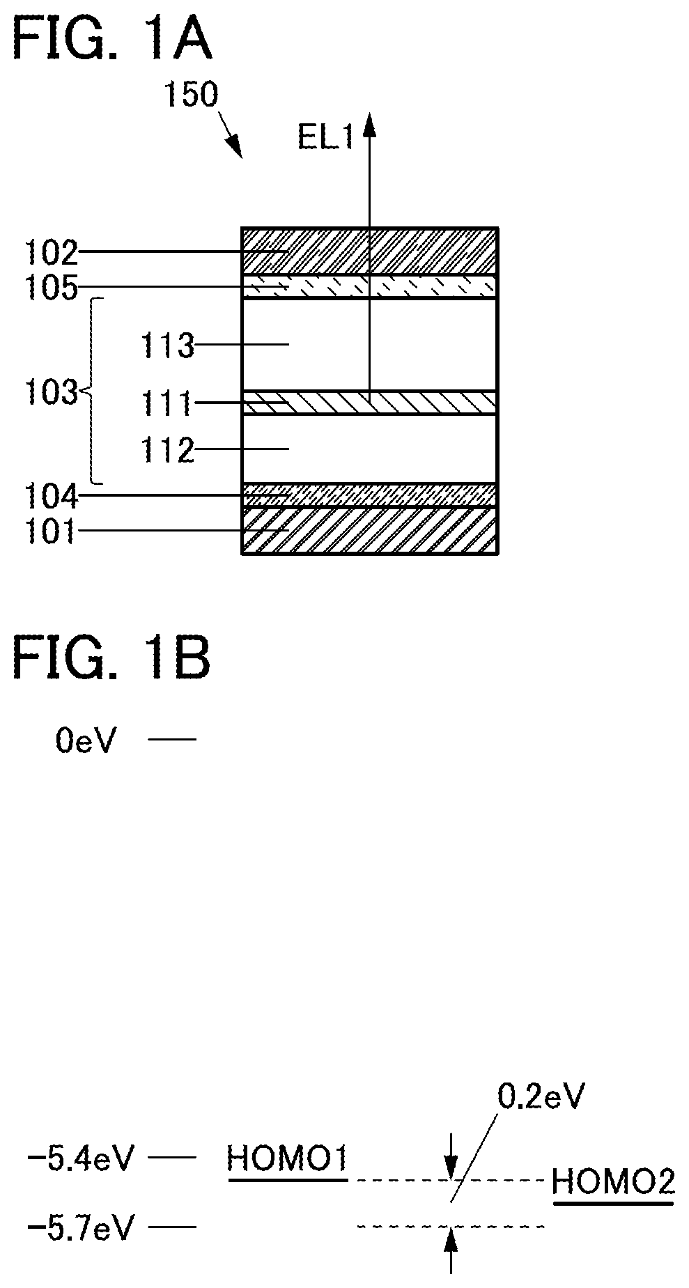
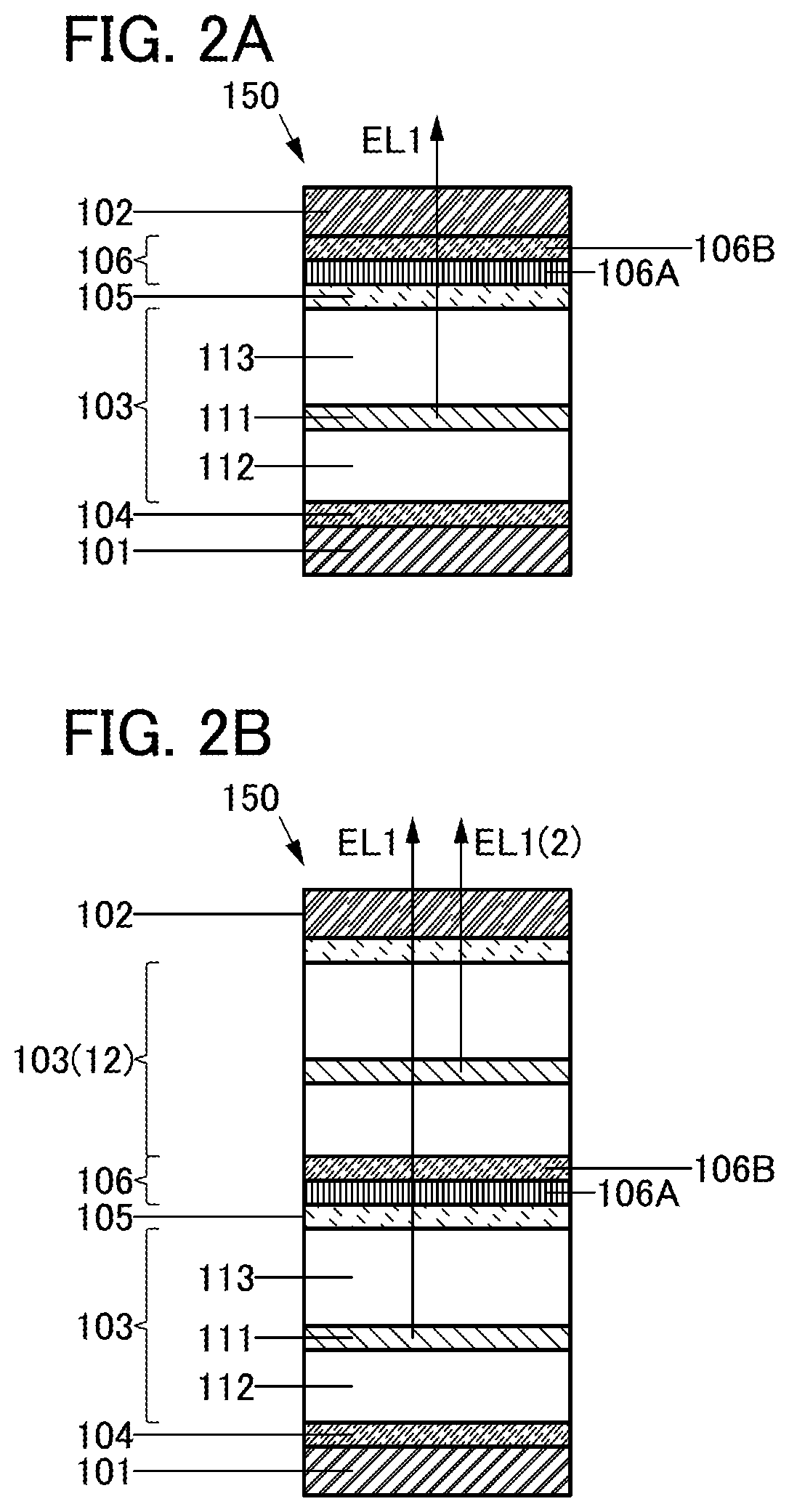
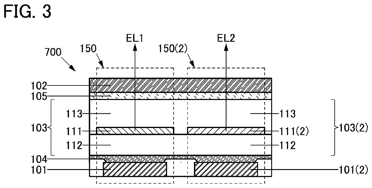
[0143]In this embodiment, a structure of a light-emitting device 150 of one embodiment of the present invention will be described with reference to FIGS. 1A and 1B.
150>
[0144]The light-emitting device 150 described in this embodiment includes an electrode 101, an electrode 102, and a unit 103. The electrode 102 includes a region overlapping with the electrode 101 and the unit 103 includes a region between the electrode 101 and the electrode 102.
STRUCTURE EXAMPLE OF UNIT 103
[0145]The unit 103 has a single-layer structure or a stacked-layer structure. The unit 103 includes a layer 111, a layer 112, and a layer 113, for example (see FIG. 1A).
[0146]The layer 111 includes a region between the layer 112 and the layer 113, the layer 112 includes a region between the electrode 101 and the layer 111, and the layer 113 includes a region between the electrode 102 and the layer 111.
[0147]The unit 103 can include, for example, a layer selected from functional layers such as a light-emitting layer...
embodiment 3
[0181]In this embodiment, a structure of the light-emitting device 150 of one embodiment of the present invention is described with reference to FIGS. 1A and 1B.
STRUCTURE EXAMPLE OF LIGHT-EMITTING DEVICE 150>
[0182]The light-emitting device 150 described in this embodiment includes the electrode 101, the electrode 102, the unit 103, and the layer 104. The electrode 102 includes a region overlapping with the electrode 101, and the unit 103 includes a region between the electrode 101 and the electrode 102. The layer 104 includes a region between the electrode 101 and the unit 103. For example, the structure described in Embodiment 2 can be employed for the unit 103.
STRUCTURE EXAMPLE OF ELECTRODE 101
[0183]For example, a conductive material can be used for the electrode 101. Specifically, a metal, an alloy, a conductive compound, and a mixture of these, or the like can be used for the electrode 101. For example, a material having a work function higher than or equal to 4.0 eV can be suit...
PUM
 Abstract
Description
Claims
Application Information
 - R&D
- Intellectual Property
- Life Sciences
- Materials
- Tech Scout
- Unparalleled Data Quality
- Higher Quality Content
- 60% Fewer Hallucinations
Browse by: Latest US Patents, China's latest patents, Technical Efficacy Thesaurus, Application Domain, Technology Topic, Popular Technical Reports.
© 2025 PatSnap. All rights reserved.Legal|Privacy policy|Modern Slavery Act Transparency Statement|Sitemap|About US| Contact US: help@patsnap.com